Plate object dividing device

A ring-shaped frame and wafer technology, which is applied to fine working devices, stone processing equipment, manufacturing tools, etc., can solve the problems of time-consuming segmentation and poor productivity.

Active Publication Date: 2015-05-13
DISCO CORP
View PDF14 Cites 0 Cited by
  • Summary
  • Abstract
  • Description
  • Claims
  • Application Information

AI Technical Summary

Problems solved by technology

[0013] However, although the wafer dividing device disclosed in the above-mentioned Patent Document 4 can accurately and reliably divide the wafer along the planned dividing line formed with the starting point of fracture, the dividing process has to be performed for each planned dividing line formed with the starting point of breaking, and there is a problem. Segmentation takes time and poor productivity

Method used


Image

  • Plate object dividing device
  • Plate object dividing device
  • Plate object dividing device

Examples


Embodiment Construction

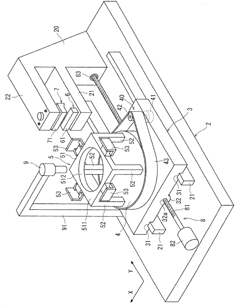
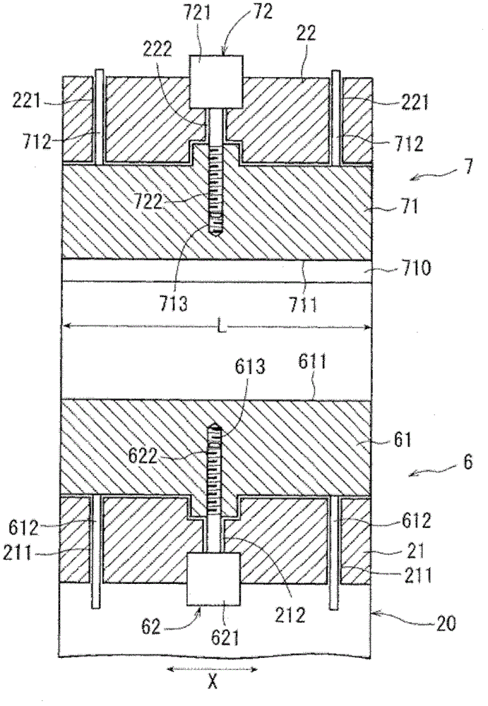
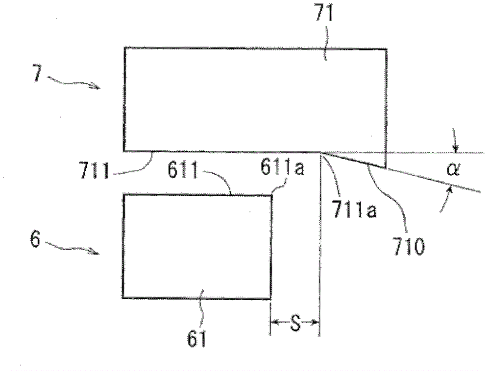
[0035]Hereinafter, preferred embodiments of the plate-shaped object dividing device configured according to the present invention will be described in detail with reference to the drawings.

[0036] First, refer to Figure 5 to Figure 9 A plate-shaped object having a fracture origin formed along a planned dividing line formed parallel to the surface as a workpiece will be described.

[0037] Figure 5 A perspective view is shown of an optical device wafer as a plate-shaped object divided by the plate-shaped object dividing apparatus according to the present invention. Figure 5 The optical device wafer 10 shown is composed of, for example, a sapphire wafer with a thickness of 100 μm, and a plurality of parallel dividing lines 101 are formed in a grid pattern on the surface 10 a. In addition, on the surface 10a of the optical device wafer 10, light-emitting diodes and laser diodes formed by laminating gallium nitride-based compound semiconductors and the like are formed in a ...


PUM

PropertyMeasurementUnit
thicknessaaaaaaaaaa

Abstract

The invention provides a plate object dividing device, capable of accurately and reliably dividing the plate object such as a wafer along a dividing predetermining line. The plate object dividing device divides the plate object adhered on the surface of an adhering band along the dividing predetermining line and is provided with a frame maintaining member; a first plate object supporting member which has a first supporting member and a first positioning mechanism, wherein the first maintaining member has a guide surface acting on the back surface of the adhering band and the first positioning mechanism positions the first supporting member at an acting position and a withdrawing position where the back surface of the adhering band is affected; a second plate object supporting member having a second supporting member and a second positioning mechanism, wherein the second supporting member has a guiding surface and a pressing surface acting on the upper surface of the plate object and the second positioning mechanism positions the second supporting member at the acting position and the withdrawing position where upper surface of the plate object is affect; and a moving member driving the frame maintaining member to relatively move in the direction orthogonal to the edge of the guide surface.

Description

technical field [0001] The present invention relates to a dividing device for dividing a plate-like object such as a semiconductor wafer along a predetermined dividing line. Background technique [0002] In the manufacturing process of a semiconductor device, a plurality of regions are divided by dividing lines arranged in a grid on the surface of a roughly disc-shaped semiconductor wafer, and ICs (Integrated Circuits) are formed in the divided regions. , LSI (large scale integration: large scale integrated circuit) and other devices. Next, the semiconductor wafer is divided along planned division lines to manufacture individual semiconductor devices. [0003] In addition, in the optical device manufacturing process, an optical device layer made of a gallium nitride-based compound semiconductor is laminated on the surface of a sapphire substrate or a silicon carbide substrate, and a plurality of optical device layers divided by a plurality of dividing lines formed in a grid...

Claims


Application Information

Patent Timeline
Patent Type & Authority Patents(China)
IPC IPC(8): B28D5/04
Inventor 相川力吉田博斗
Owner DISCO CORP
Why Eureka
Try Eureka