Processing method of wafer

A processing method and wafer technology, applied in the manufacturing of electrical components, electric solid-state devices, semiconductor/solid-state devices, etc., can solve the problems of shortening the processing time, reducing the spacer, and spending the processing time, so as to shorten the processing time, reduce the The effect of spacer, efficient fracture

Pending Publication Date: 2020-03-31
DISCO CORP
View PDF7 Cites 0 Cited by
  • Summary
  • Abstract
  • Description
  • Claims
  • Application Information

AI Technical Summary

Problems solved by technology

[0008] In plasma etching, the so-called BOSCH method is widely used, and it is suitable for realizing vertical deep processing of wafers at high speed and with a desired aspect ratio (for example, refer to Patent Document 3). However, for the etching gas used in the BOSCH method, there are The problem that DAF is not easily etched or not etched
[0009] In addition, a device for breaking DAF by expansion has been proposed (for example, refer to Patent Document 4), but when the chip size is reduced to, for example, several millimeters or less, there is a problem that it is not easy to separate by expansion.
[0010] It is also considered to use a laser processing device to disconnect the DAF, but there are the following problems: In a wafer with a small chip size, there are many lines to be laser processed, which takes processing time and reduces efficiency.
[0011] Accordingly, when dividing a wafer on which a die attach layer (DAF) is stacked on the back surface, there is a problem in that the die attach layer can be efficiently divided while reducing the spacer and shortening the processing time. open

Method used


Image

  • Processing method of wafer
  • Processing method of wafer
  • Processing method of wafer

Examples


Embodiment approach 1

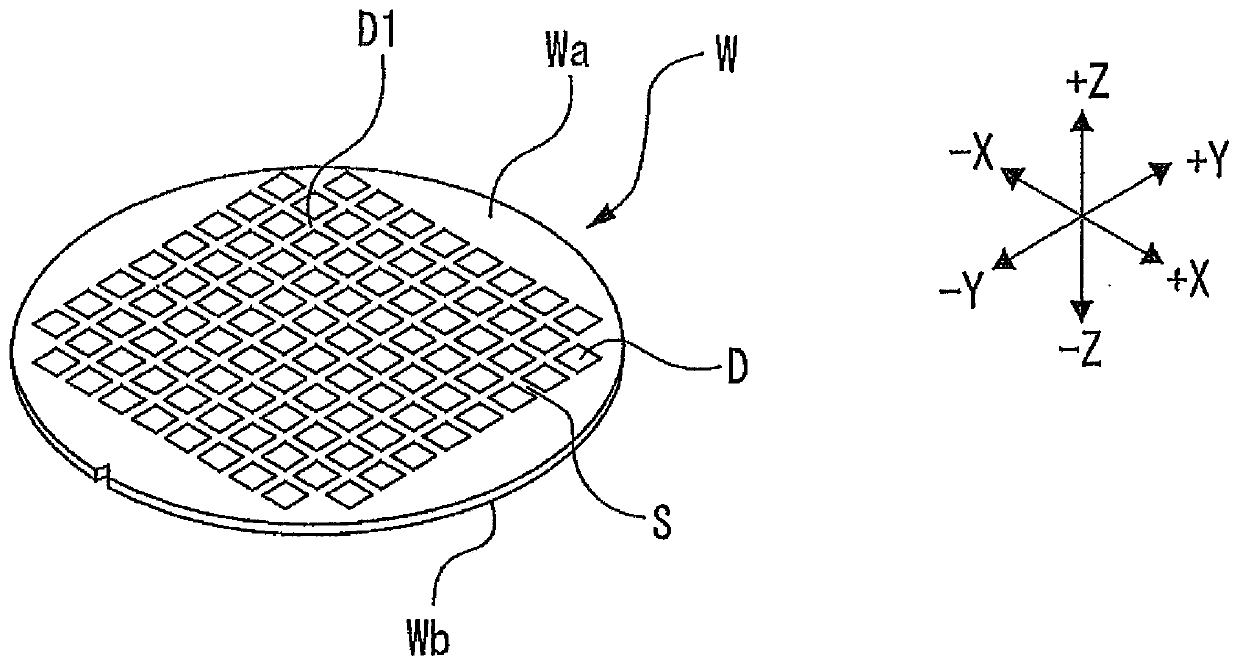
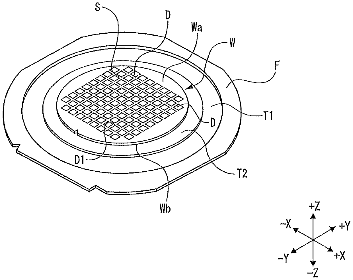
[0038] Hereinafter, the wafer processing method of the present invention (the processing method of the first embodiment) will be described figure 1 Each step of the processing method when the illustrated wafer W is divided into chips having devices D will be described.

[0039] The wafer W is, for example, a semiconductor wafer with a circular outer shape using silicon as a base material. Its front surface Wa is divided into a grid by a plurality of vertical dividing lines S, and ICs and other devices are formed in each area divided into the grid. D. In addition, for example, a device layer D1 is laminated on the planned dividing line S. The device layer D1 includes a circuit layer made of metal and an insulating layer (for example, a low-k film) that insulates the circuits.

[0040] In addition to silicon, the wafer W may also be made of gallium arsenide, sapphire, gallium nitride, silicon carbide, or the like.

[0041] (1) Piece pasting steps

[0042] In the wafer processing method...

Embodiment approach 2

[0115] Hereinafter, the wafer processing method (the processing method of Embodiment 2) implementing the present invention will be described figure 1 Each step of the processing method when the illustrated wafer W is divided into chips having devices D will be described.

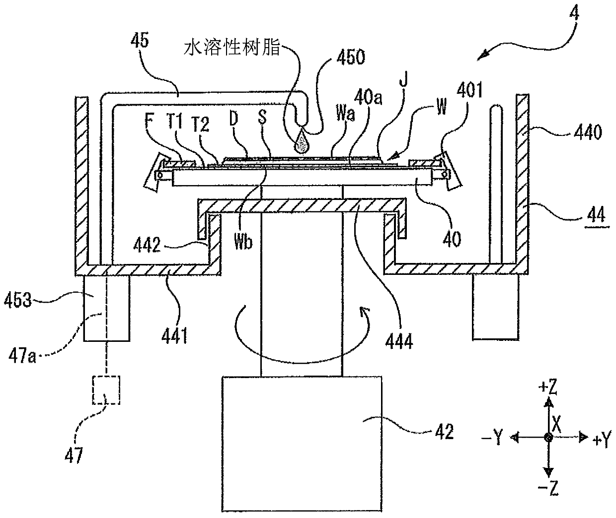
[0116] (1-1) Application of water-soluble resin to the wafer in the wafer dividing step

[0117] In the wafer processing method of this embodiment 2, firstly figure 1 The wafer W shown is transported to Picture 11 The spin coater 4 shown. In addition, before being transferred to the spin coater 4, a protective tape (not shown) is attached to the front surface Wa of the wafer W. Then, the wafer W is sucked and held by the holding table 40 with the front Wa side to which the protective tape is pasted, and the holding table 40 holding the wafer W is lowered to the coating height position in the housing 44. In addition, the supply port 450 of the nozzle 45 is positioned above the center of the wafer W.

[0118] Next...


PUM


Abstract

Provided is a wafer processing method for dividing a wafer in which a chip mounting layer is laminated on the back surface, reducing the number of separation channels, shortening the processing time,and efficiently breaking the chip mounting layer. The wafer processing method includes: a wafer dividing step of performing plasma etching on a wafer (W) with a mask (J1) having an opening along a planned dividing line (S) interposed therebetween, and dividing the wafer to form chips (C); a sheet attaching step of laminating a chip mounting layer (T2) on the back surface (Wb) of the wafer before or after the wafer dividing step is performed, and attaching the wafer to the expansion sheet (T1) with the chip mounting layer interposed therebetween; a solvent providing step of providing a solventfor degrading the chip mounting layer between adjacent chips from the front surface (Wa) side of the wafer after the wafer dividing step and the wafer pasting step are performed, and degrading the chip mounting layer exposed between the chips; and a breaking step of breaking the chip mounting layer along the etching groove (M) by expanding the expansion sheet after the solvent supply step is performed.

Description

Technical field [0001] The present invention relates to a method for processing a wafer having a die attach layer laminated on the back surface. Background technique [0002] In order to reduce the width of the spacer channel (pre-divided line) set on the front side (decrease the spacer channel) and increase the number of chips per wafer and to shorten the processing time, so-called plasma cutting has been used in the past. The wafer of the workpiece is divided (for example, refer to Patent Document 1). [0003] In addition, in order to mount a semiconductor chip formed by dividing a semiconductor wafer on a mounting substrate, there is a technique of attaching a DAF (Die Attach Film) to the back surface of the semiconductor wafer in advance. In the adhesive film of, the chip is bonded to the mounting substrate via the adhesive film on the back surface of the divided chip (for example, refer to Patent Document 2). In this technology, DAF is attached to the wafer before the wafer ...

Claims


Application Information

Patent Timeline
Patent Type & Authority Applications(China)
IPC IPC(8): H01L21/78H01L21/3065H01L21/308H01L21/683
CPCH01L21/78H01L21/3065H01L21/3081H01L21/3085H01L21/6836H01L2221/68327H01L21/76H01L24/86H01L21/02076
Inventor 铃木稔
Owner DISCO CORP
Why Eureka
Try Eureka