

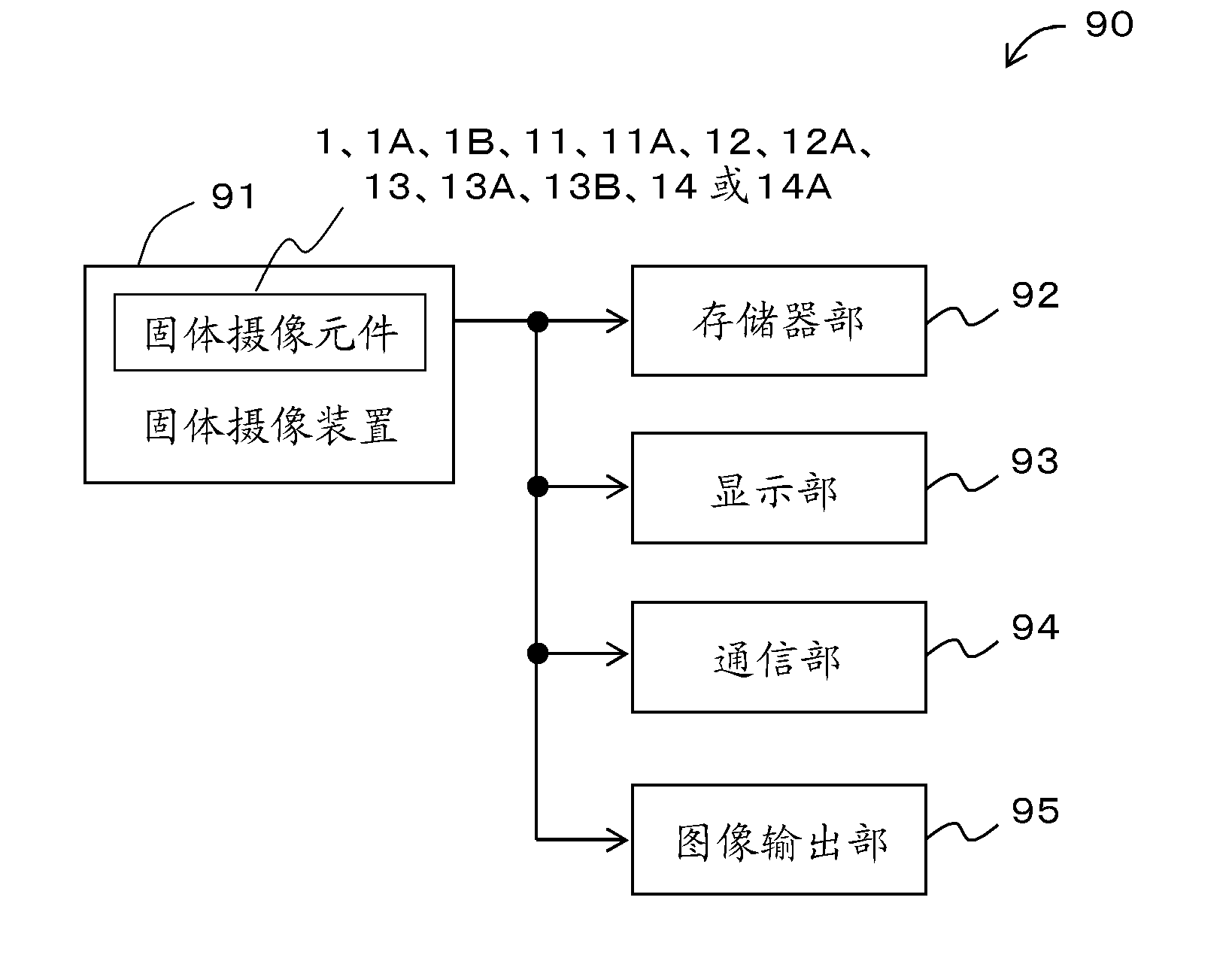
Solid-state imaging devices and electronic information equipment
A solid-state imaging element and semiconductor technology, which is applied in the direction of electric solid-state devices, electrical components, semiconductor devices, etc., can solve the problem of not being able to effectively suppress color mixing, and achieve the effects of suppressing color mixing, high light-receiving sensitivity, and high light-receiving sensitivity
- Summary
- Abstract
- Description
- Claims
- Application Information
AI Technical Summary
Problems solved by technology
Method used
Image

Examples
Embodiment approach 1
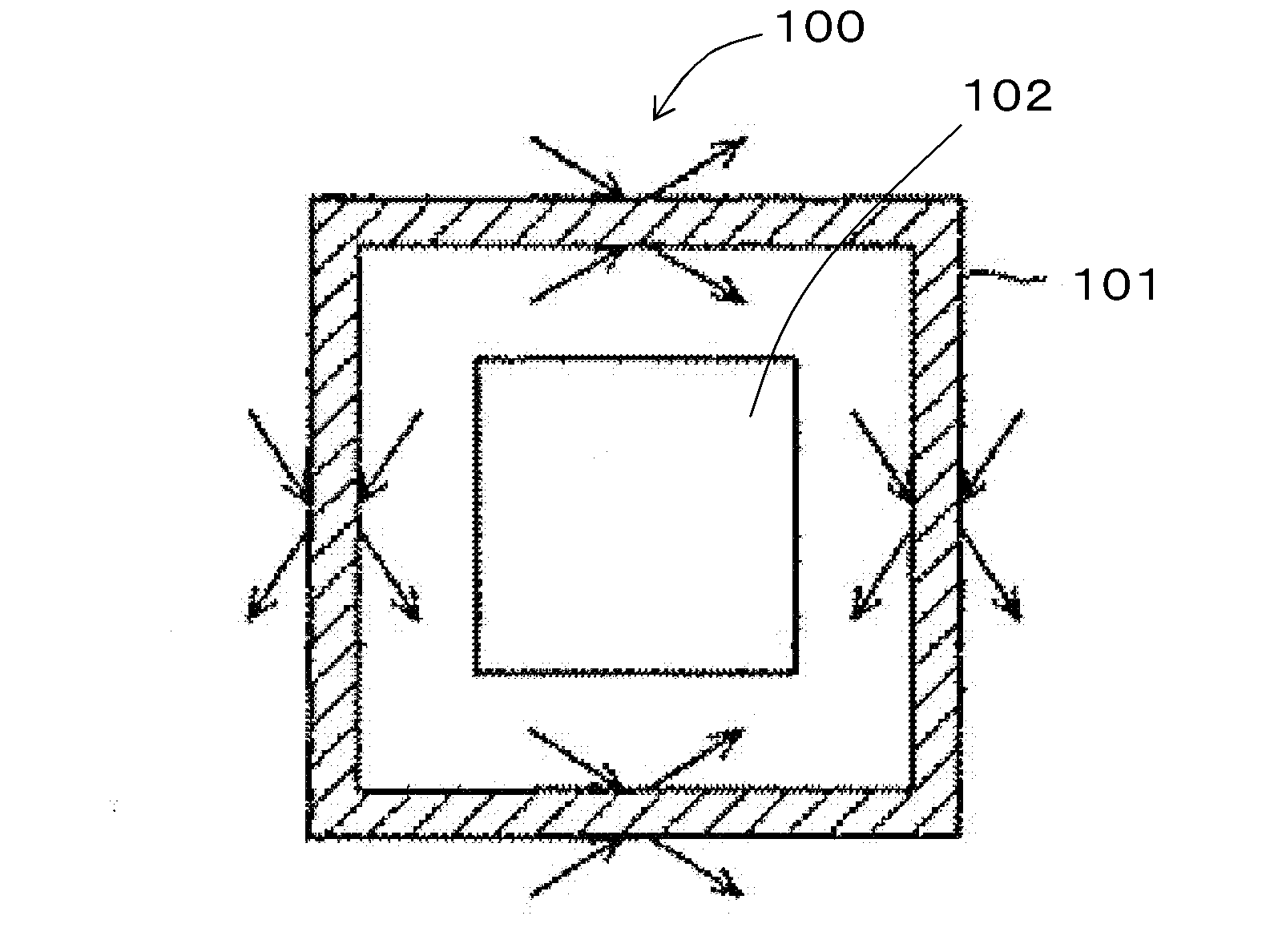
[0071] figure 1 It is a vertical cross-sectional view showing a configuration example of main parts of the solid-state imaging device according to Embodiment 1 of the present invention.
[0072] like figure 1 As shown, in the solid-state imaging device 1 of the first embodiment, on the upper part of the semiconductor substrate 2, a plurality of semiconductor elements configured to perform photoelectric conversion of image light from a subject and perform imaging are arranged in a matrix. a light receiving unit 3 . Above each light-receiving portion 3, corresponding to each light-receiving portion 3, a planarizing film 4 is interposed, and a transparent film 10 (SiO 2 film) are provided with respective color filters 5a, 5b. Above the color filters 5 a , 5 b , corresponding to the light receiving portions 3 , there are provided microlenses 7 for condensing incident light on the light receiving portions 3 via the planarizing film 6 . The color filters 5a and 5b are any one ...
Embodiment approach 2
[0081] In this Embodiment 2, between the light-shielding wall 8 (or reflective wall) and the color filters 5a, 5b embedded therebetween, a transparent film for bonding them (for example, a metal and an organic film) is provided. The case of bonding the film will be described.
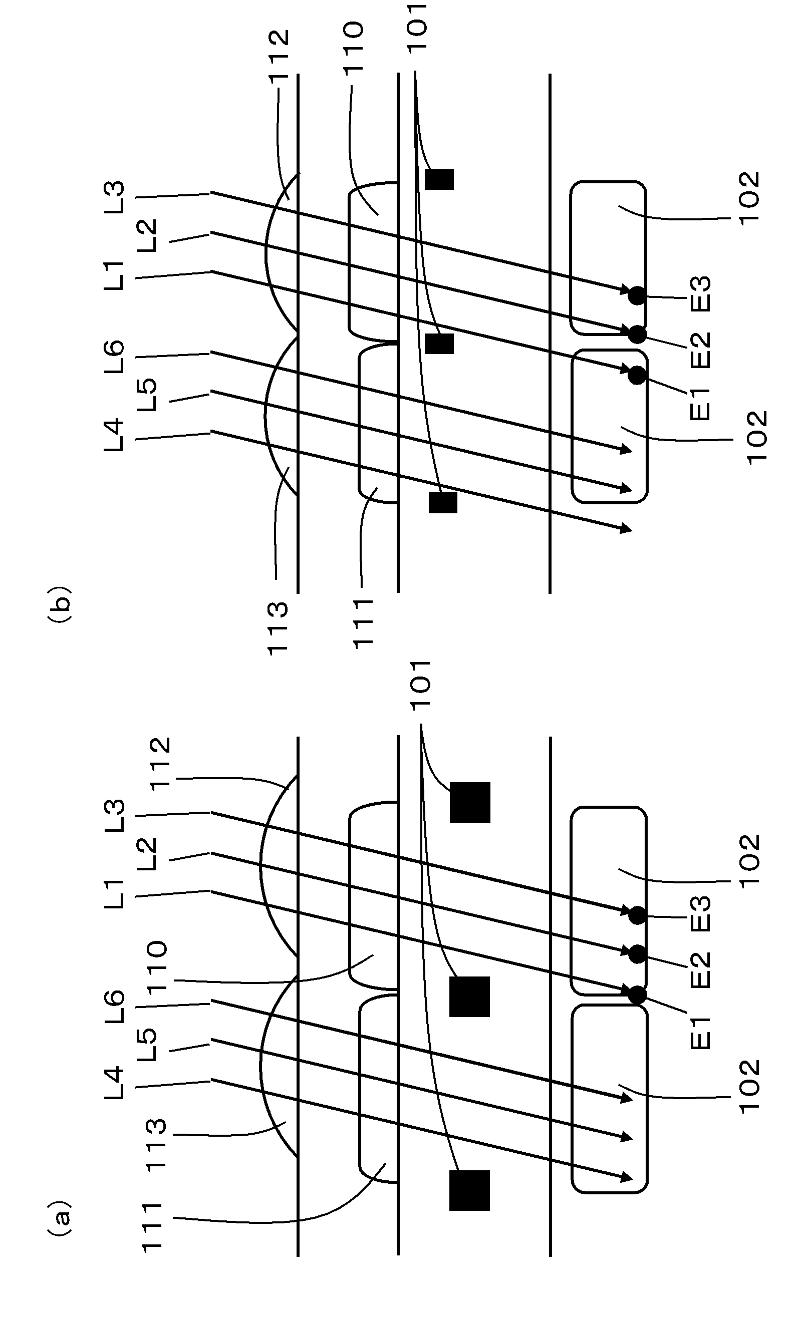
[0082] Figure 4 It is a longitudinal sectional view showing a configuration example of main parts of the solid-state imaging device according to Embodiment 2 of the present invention, (a) is a longitudinal sectional view showing a case where the bonding film is discontinuous, and (b) is a longitudinal sectional view showing a case where the bonding film is continuous. Sectional view.
[0083] like Figure 4 As shown in (a), in the solid-state imaging device 11 according to the second embodiment, semiconductor elements for performing photoelectric conversion of image light from a subject to take an image are arranged in a matrix on the upper portion of the semiconductor substrate 2 . A plurality of l...
Embodiment approach 3
[0091] In Embodiment 3, a case where the light-shielding wall 8 (or reflective wall) and / or the color filters 5 a and 5 b are directly provided on the semiconductor substrate 2 will be described.
[0092] Figure 5 It is a vertical cross-sectional view showing a configuration example of main parts of a solid-state imaging device according to Embodiment 3 of the present invention.
[0093] like Figure 5 As shown, in the solid-state imaging device 12 according to the third embodiment, on the upper part of the semiconductor substrate 2, a plurality of semiconductor elements configured to perform photoelectric conversion of image light from a subject and perform imaging are arranged in a matrix. a light receiving unit 3 . On the semiconductor substrate 2 on which the light receiving portions 3 are formed, the color filters 5 a , 5 b are provided directly (without interposing the planarizing film 4 ) corresponding to the light receiving portions 3 via the transparent film 10 . ...
PUM
 Abstract
Description
Claims
Application Information