A wafer position detection device
A detection device, wafer technology, applied in electrical components, semiconductor/solid-state device manufacturing, circuits, etc., can solve problems such as damage to wafers, easy to forget to push, etc.
- Summary
- Abstract
- Description
- Claims
- Application Information
AI Technical Summary
Problems solved by technology
Method used
Image

Examples
Embodiment Construction
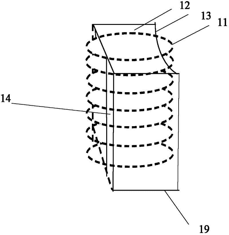
[0021] The embodiment of the present invention provides a wafer position detection device, which is used to detect the relative position of the wafer and the open wafer cassette, avoiding the edge of the wafer in the open wafer cassette from colliding with the open wafer The second side edge of the box solves the problem that the wafers are damaged before the mechanical arm drives the manipulator into the open wafer box and the wafers in the open wafer box are loaded out.
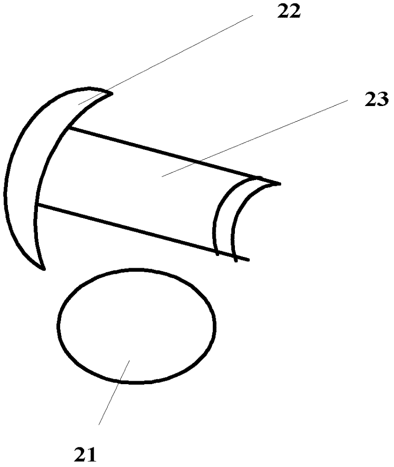
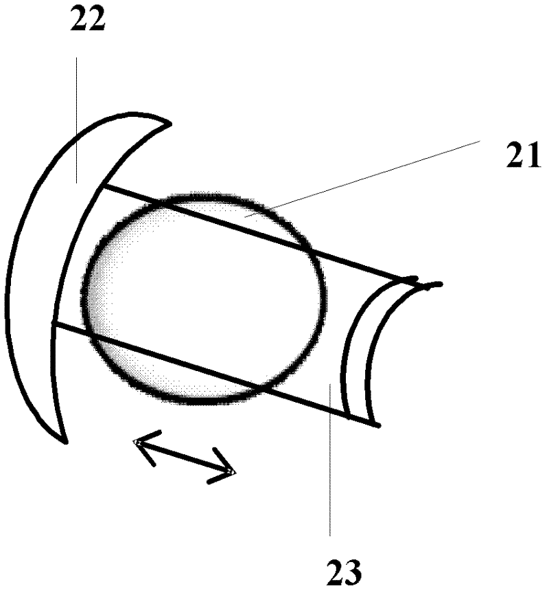
[0022] The wafer position detecting device according to the embodiment of the present invention includes: a pusher and a wafer box placed on the pusher, the wafer box has a first side for picking and placing wafers and is opposite to the first side The second side of the wafer position calibration device also includes a detection sensor, the detection sensor is composed of two parts, a signal transmitter and a signal receiver, and the signal transmitter and the signal receiver are respectively located on the...
PUM
 Abstract
Description
Claims
Application Information