Optimizing method of analogue integrated circuit design

An optimization method and integrated circuit technology, applied in computing, electrical digital data processing, instruments, etc., can solve the problems of sensitivity to parasitic effects of analog integrated circuits, failure to consider connection parasitic effects, long design cycle, etc., to improve optimization speed, Effects of shortening the design cycle and improving reliability

Active Publication Date: 2012-01-11
INST OF MICROELECTRONICS CHINESE ACAD OF SCI
View PDF1 Cites 18 Cited by
  • Summary
  • Abstract
  • Description
  • Claims
  • Application Information

AI Technical Summary

Problems solved by technology

[0003] Because the performance of analog integrated circuits is very sensitive to parasitic effects, there are such problems in existing methods: the parasitic effects between wiring, between wiring, between wiring and devices, and between devices and devices are not considered. There is a big difference between the evaluation value and the actual circuit

Method used


Image

  • Optimizing method of analogue integrated circuit design
  • Optimizing method of analogue integrated circuit design
  • Optimizing method of analogue integrated circuit design

Examples


Embodiment Construction

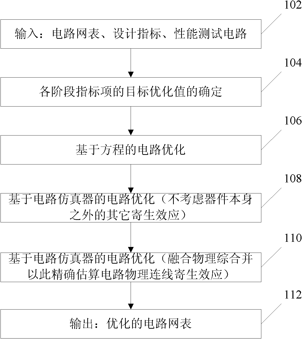
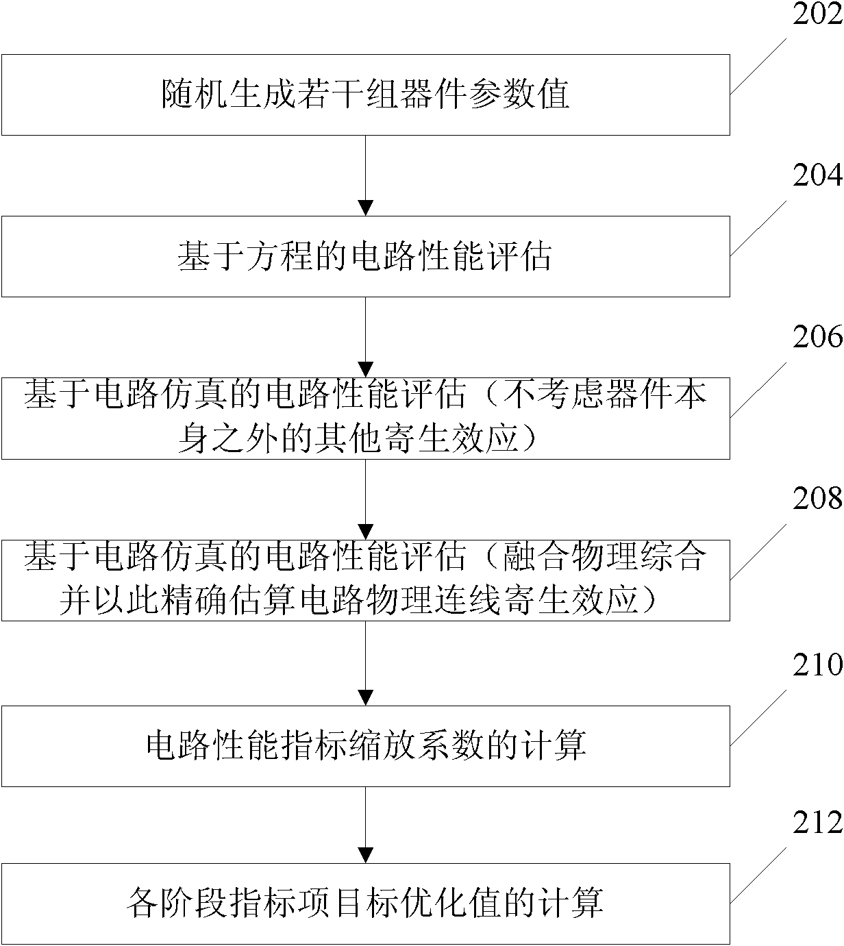
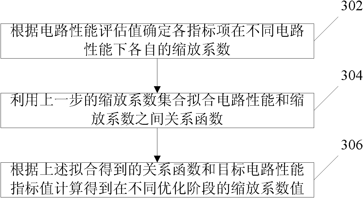
[0031] The present invention proposes a computer-aided automatic optimization method aimed at improving work efficiency for analog integrated circuit design, which specifically includes: determining the target optimization value of the circuit index item at each optimization stage before the analog circuit design optimization, using the method based on The circuit optimization method based on the equation realizes the circuit optimization of the first stage, and the circuit optimization method based on the circuit simulator that does not consider the connection parasitic effect realizes the circuit optimization of the second stage, and uses the fusion of physical synthesis and accurate estimation of the parasitic effect of the physical connection of the circuit The circuit optimization method based on circuit simulator realizes the third stage of circuit optimization. In particular, circuit optimization is controlled by using respective target optimization values ​​of circuit p...


PUM


Abstract

The invention relates to an optimizing method of an analogue integrated circuit design, belonging to the field of automation of integrated circuit designs. The optimizing method comprises the following steps of: inputting a circuit network table, performance design indexes and a performance test circuit; determining a target optimization value of each index item of circuit optimization based on an equation, an optimization value of each index item of the circuit optimization based on a circuit simulator after eliminating the self parasitic effect of a device, and an optimization value of eachindex project of the circuit optimization based on the circuit simulator after taking the physical connection parasitic effect of the circuit into account; executing the circuit optimization based onthe equation; executing the circuit optimization based on the circuit simulator; and carrying out the circuit optimization based on the circuit simulator. According to the optimizing method of the analogue integrated circuit design disclosed by the invention, the reliability of circuit evaluation is improved, and the optimization speed is increased, thus the zone times between the circuit design and the physical design is reduced, the design efficiency is improved and the design cycle is shortened.

Description

technical field [0001] The invention relates to the field of integrated circuit design automation, in particular to an analog integrated circuit design optimization method. Background technique [0002] The main methods of analog integrated circuit design optimization are: the designer manually modifies the device size according to the design experience, and then evaluates the circuit performance with the help of circuit simulation tools; establishes the circuit equation, and uses various optimization algorithms to solve the equation to obtain the parameter value of the device; Randomly change the device parameter value under the control of the circuit simulation tool to obtain the circuit performance value. In the optimization process, the device parameter value of the circuit is finally obtained. [0003] Because the performance of analog integrated circuits is very sensitive to parasitic effects, there are such problems in existing methods: the parasitic effects between w...

Claims


Application Information

Patent Timeline
IPC IPC(8): G06F17/50
Inventor 吴玉平陈岚叶甜春
Owner INST OF MICROELECTRONICS CHINESE ACAD OF SCI
Why Eureka
Try Eureka