
Structure with alignment mark and manufacture method for stacking device

A technology for alignment marks and manufacturing methods, which is applied in the field of semiconductor technology and its formed structures, can solve problems such as hindering device operation, and achieve the effects of increasing production capacity, improving technology, and relieving stress and strain

Active Publication Date: 2013-09-11
TAIWAN SEMICON MFG CO LTD
View PDF6 Cites 0 Cited by
  • Summary
  • Abstract
  • Description
  • Claims
  • Application Information

AI Technical Summary

Problems solved by technology

Misalignment between film layers hinders device operation

Method used


Image

  • Structure with alignment mark and manufacture method for stacking device
  • Structure with alignment mark and manufacture method for stacking device
  • Structure with alignment mark and manufacture method for stacking device

Examples


Embodiment Construction

[0029] The manufacture and use of the embodiments of the present invention are described below. It should be readily appreciated, however, that the embodiments of the invention provide many suitable inventive concepts that can be implemented in a wide variety of specific contexts. The specific embodiments disclosed are only used to illustrate the making and use of the present invention in specific ways, and are not intended to limit the scope of the present invention.

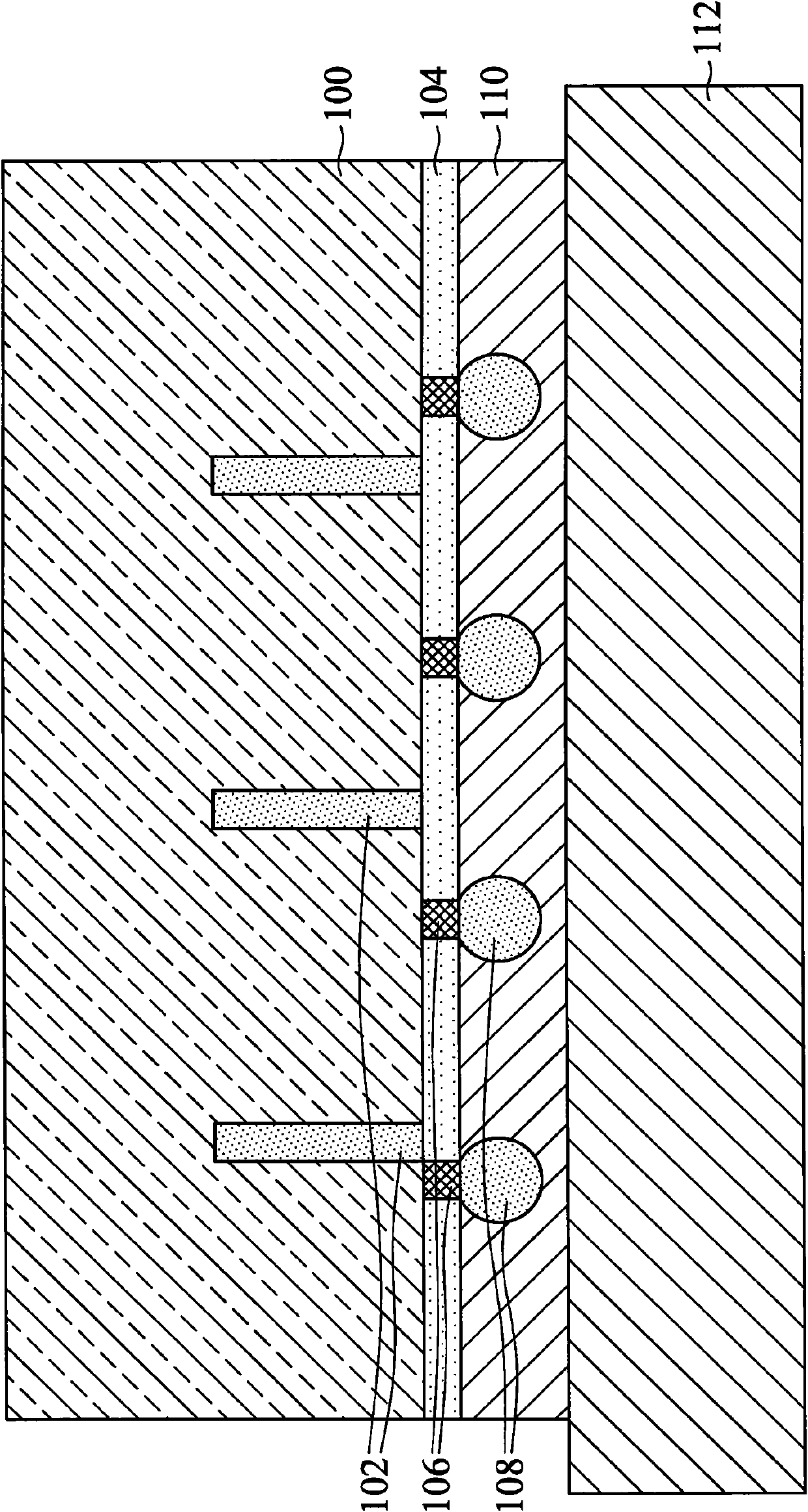
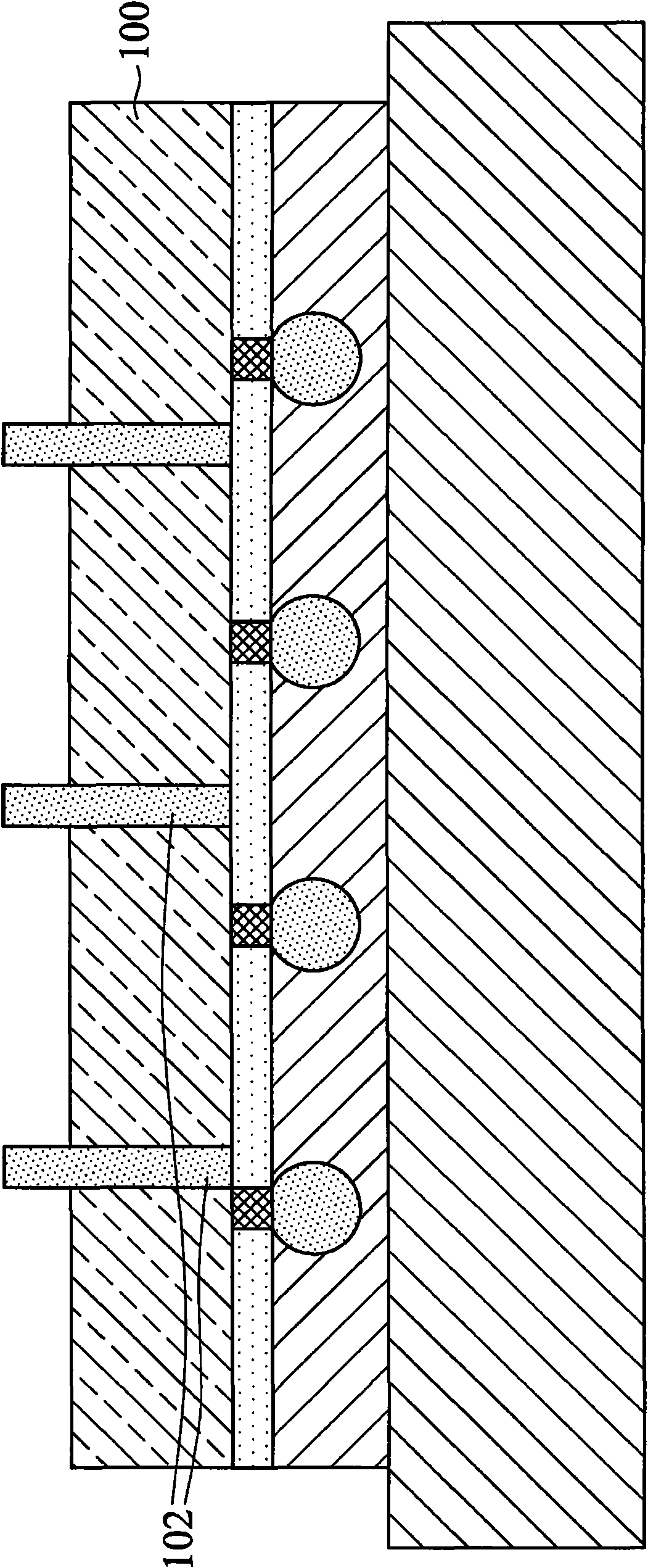
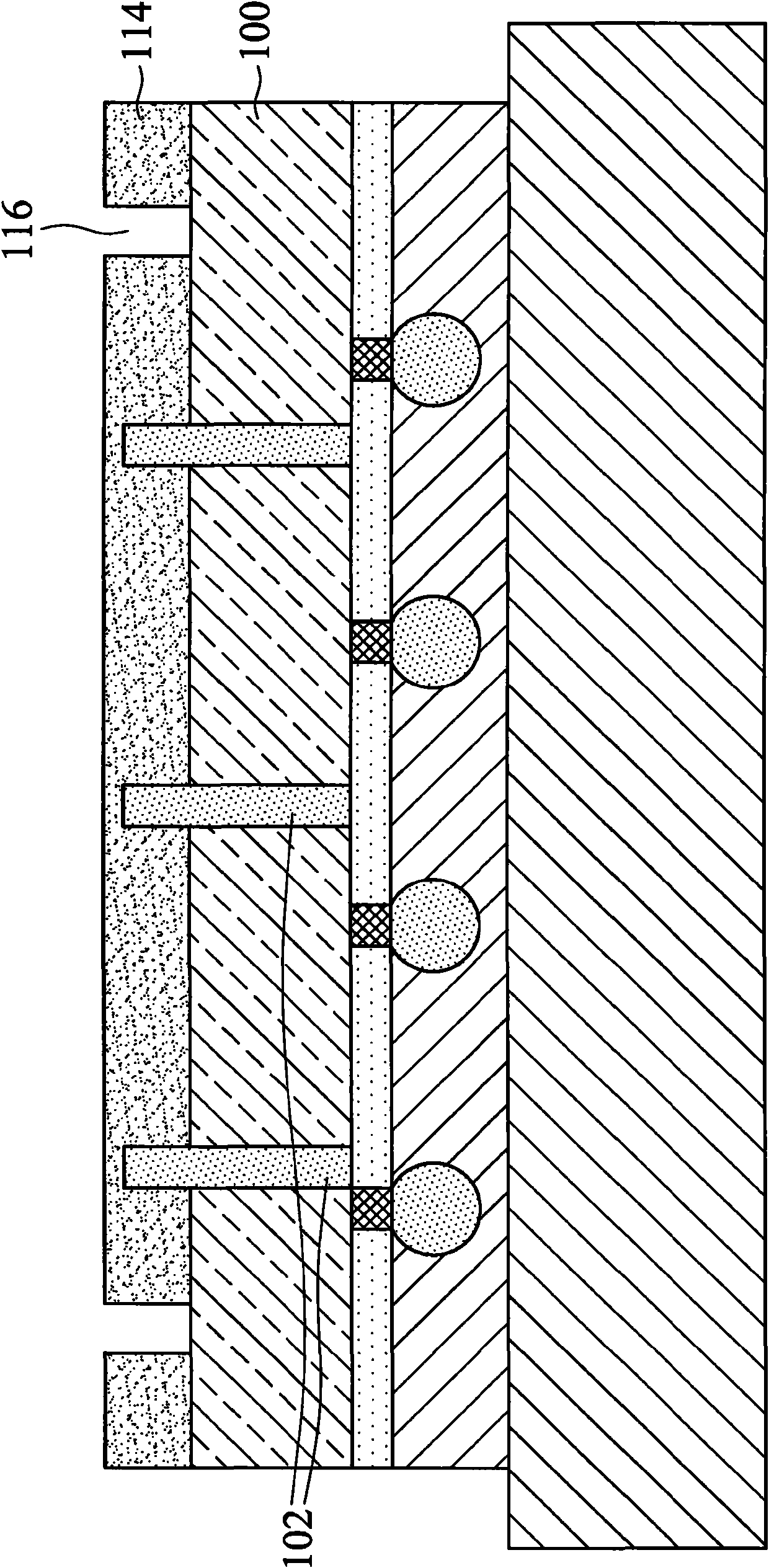
[0030] A specific background of embodiments of the present invention is described below, that is, alignment marks formed during processing of chips in a stacked device. However, the above-described embodiments are also applicable to an interposer or another structure that uses alignment marks during processing.

[0031] Figure 1A to Figure 1H A method for manufacturing an alignment mark for a stacked device according to an embodiment of the present invention is presented. figure 2 shown by Figure 1A to Fig...


PUM


Abstract

In accordance with an embodiment, a structure comprises a substrate having a first area and a second area; a through substrate via (TSV) in the substrate penetrating the first area of the substrate; an isolation layer over the second area of the substrate, the isolation layer having a recess; and a conductive material in the recess of the isolation layer, the isolation layer being disposed between the conductive material and the substrate in the recess.

Description

technical field [0001] The present invention relates to a semiconductor process and its formed structure, in particular to an alignment mark manufacturing method and its formed structure. Background technique [0002] In semiconductor processing, the fabrication of structures and devices typically involves sequentially forming one layer of material or composition of materials on top of another. These layers are usually etched or doped using lithography to control the etched or doped regions. For example, forming the source / drain of a transistor may include forming a photoresist layer on a semiconductor substrate in which the source / drain regions are formed. The photoresist layer is exposed such that the photoresist layer over the source / drain regions is removed. The semiconductor layer is doped with a photoresist layer to prevent the unexposed regions from being doped. Moreover, the contact window (contact) of the source / drain region may include: depositing an insulating ...

Claims


Application Information

Patent Timeline
Patent Type & Authority Patents(China)
IPC IPC(8): H01L23/544H01L21/00G03F9/00
CPCH01L21/6835H01L2223/54426H01L2221/68327H01L23/544H01L2224/13H01L21/76898H01L21/30604H01L21/76831H01L21/76877H01L23/481
Inventor 蔡承祐王势辉邱建明陈嘉和蔡方文吴文进林俊成邱文智郑心圃余振华
Owner TAIWAN SEMICON MFG CO LTD
Learn More