
Multiplication-type A/D (Analog/Digital) converter capable of correcting limited gain error
A digital-to-analog converter and limited-gain technology, which is applied in the field of high-speed, high-precision, low-power pipeline A/D converters, can solve the problem of low-power multiplying digital-to-analog converters with limited gain errors that are difficult to reduce, operational amplifier DC Gain limitation, equivalent non-ideality of virtual ground, etc., to achieve the effect of reducing DC gain requirements, reducing power consumption, and reducing power consumption
- Summary
- Abstract
- Description
- Claims
- Application Information
AI Technical Summary
Problems solved by technology
Method used
Image

Examples
Embodiment Construction
[0024] The specific implementation manners of the present invention are not limited to the following description, and are now further described in conjunction with the accompanying drawings.
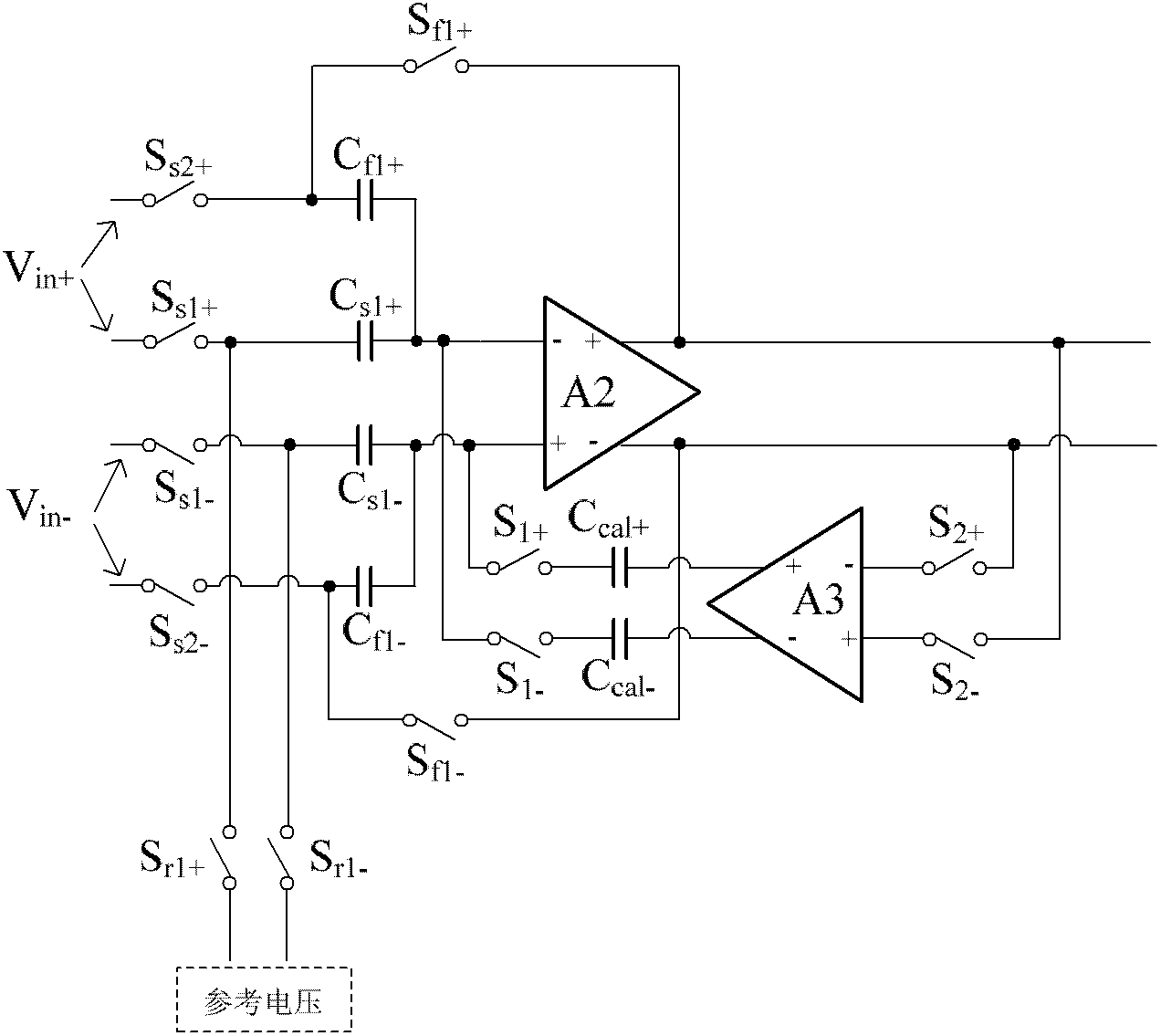
[0025] The circuit diagram of the multiplying digital-to-analog converter of the present invention is as figure 2 shown. Its basic composition includes an amplifying circuit unit and a finite gain error correction circuit unit. Amplifying circuit unit includes: operational amplifier A2, sampling capacitor C s1+ and C s1- , feedback capacitance C f1+ and C f1- , Interconnect switch S s1+ and S s1- , Interconnect switch S r1+ and S r1- , Interconnect switch S f1+ and S f1- . The finite gain error correction circuit unit includes: variable gain amplifier A3, compensation capacitor C cal+ and C cal- , Interconnect switch S 1+ and S 1- , Interconnect switch S 2+ and S 2- .
[0026] figure 2 The specific connection relationship and functional relationship in are the same a...
PUM
 Abstract
Description
Claims
Application Information