Supercharge Your Innovation With Domain-Expert AI Agents!

Soft and hard circuit board and manufacturing method thereof

A manufacturing method and technology for flexible circuit boards, which are applied in multilayer circuit manufacturing, printed circuit manufacturing, structural connection of printed circuits, etc., can solve problems such as incomplete bonding, damage to circuit layers, human and environmental hazards, and avoid Harmful effect

Active Publication Date: 2013-11-20
UNIMICRON TECH CORP
View PDF4 Cites 0 Cited by
  • Summary
  • Abstract
  • Description
  • Claims
  • Application Information

AI Technical Summary

Problems solved by technology

[0004] However, during the electroplating process, because the electroplating solution used is usually toxic, it is easy to cause harm to the human body and the environment
In addition, due to the high hardness of the metal vias formed by the electroplating process, when the subsequent lamination (lamination) process is performed on the above-mentioned flexible and rigid circuit board, due to the impact of compressive stress, these metal vias and The interface between the wiring layers may be defective (such as cracks, incomplete bonding) or these metal vias may be broken
In addition, these metal vias may also be deformed due to the influence of thermal stress during the high-temperature process, so it is easy to cause damage to the circuit layer between these metal vias

Method used


Image

  • Soft and hard circuit board and manufacturing method thereof
  • Soft and hard circuit board and manufacturing method thereof
  • Soft and hard circuit board and manufacturing method thereof

Examples


Embodiment Construction

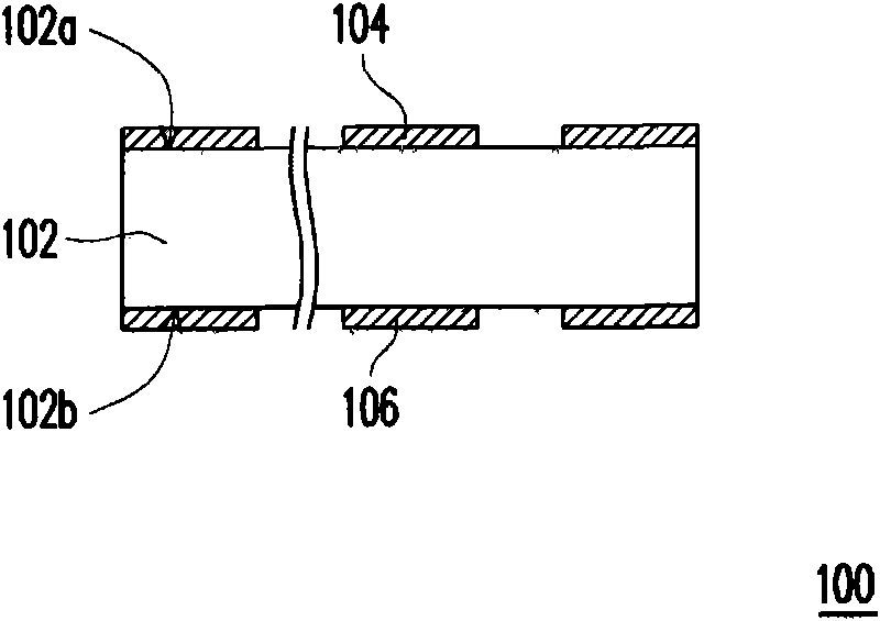
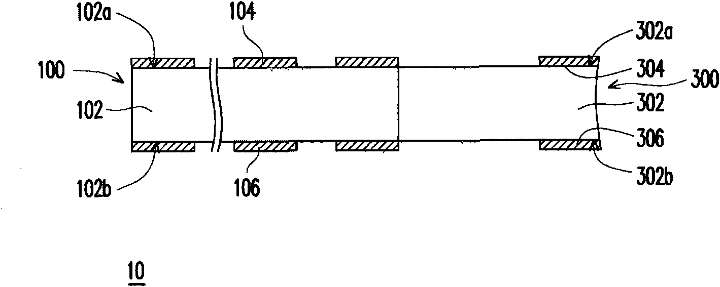
[0029] Figure 1A to Figure 1D It is a cross-sectional view of a manufacturing method of a rigid-flex circuit board according to an embodiment of the present invention. First, please refer to Figure 1A , providing a flexible printed circuit board 100 . The flexible circuit board 100 includes a dielectric layer 102 and a circuit layer 104 . The dielectric layer 102 has a surface 102a and a surface 102b opposite to the surface 102a. The material of the dielectric layer 100 is, for example, a soft dielectric material. The circuit layer 104 is disposed on the surface 102a. The material of the wiring layer 104 is copper, for example. In addition, the flexible circuit board 100 may further include a circuit layer 106 . The circuit layer 106 is disposed on the surface 102b. The material of the wiring layer 106 is copper, for example. The step of forming the flexible circuit board 100 is, for example, to form circuit material layers on the surface 102 a and the surface 102 b o...


PUM


Abstract

The invention discloses a soft and hard circuit board and a manufacturing method thereof. The soft and hard circuit board comprises a soft circuit board, a hard circuit board and a circuit structure. The soft circuit board comprises a first dielectric layer and a first circuit layer. The first dielectric layer comprises a first surface. The first circuit layer is configured on the first surface. The edge of the hard circuit board abuts against the edge of the soft circuit board. The circuit structure is configured on the soft and the hard circuit boards. The circuit structure comprises a second dielectric layer, a second circuit layer and a conductive adhesive conduction hole. The second dielectric layer is configured on the soft and the hard circuit boards and covers part of the first circuit layer. The second circuit layer is configured on the second dielectric layer. The conductive adhesive conduction hole is configured in the second dielectric layer and electrically connected with the first and the second circuit layers. An interface is arranged between the conductive adhesive conduction hole and the second circuit layer.

Description

technical field [0001] The invention relates to a flex-rigid circuit board and a manufacturing method thereof, in particular to a flex-rigid circuit board with conducting holes of conductive glue and a manufacturing method thereof. Background technique [0002] In terms of the soft and hard properties of the dielectric layer, circuit boards can be divided into rigid circuit boards (also known as hard boards), flexible circuit boards (also known as soft boards) and flexible and hard circuit boards (also known as soft and hard boards). ). [0003] Generally speaking, the manufacturing method of the flexible and rigid circuit board is to first make the edge of the flexible circuit board and the edge of the rigid circuit board adjoin. Then, a dielectric layer is formed on the flexible circuit board and the rigid circuit board, and the dielectric layer covers part of the flexible circuit board and part of the rigid circuit board. Next, a circuit material layer is formed on the ...

Claims


Application Information

Patent Timeline
Patent Type & Authority Patents(China)
IPC IPC(8): H05K1/14H05K3/00H05K3/40H05K3/46
Inventor 谢建彦张宏麟
Owner UNIMICRON TECH CORP
Features
  • R&D
  • Intellectual Property
  • Life Sciences
  • Materials
  • Tech Scout
  • Unparalleled Data Quality
  • Higher Quality Content
  • 60% Fewer Hallucinations
Learn More