Phase change memory element and manufacturing method thereof

A technology of phase change memory and components, applied in the direction of electrical components, etc., can solve the problems that the bottom electrode cannot be defined to meet the process requirements, and the contact area between the bottom electrode and the phase change layer can be reduced, so as to reduce the contact area and improve the reading and writing speed , Improve the effect of heating efficiency

Active Publication Date: 2012-03-21
SEMICON MFG INT (SHANGHAI) CORP +1
View PDF3 Cites 7 Cited by
  • Summary
  • Abstract
  • Description
  • Claims
  • Application Information

AI Technical Summary

Problems solved by technology

Usually the width of the top of the hole formed by etching is larger than the width of the bottom, resulting in the formed bottom electrode being in an inverted trumpet shape, so it is difficult to further reduce the contact area between

Method used

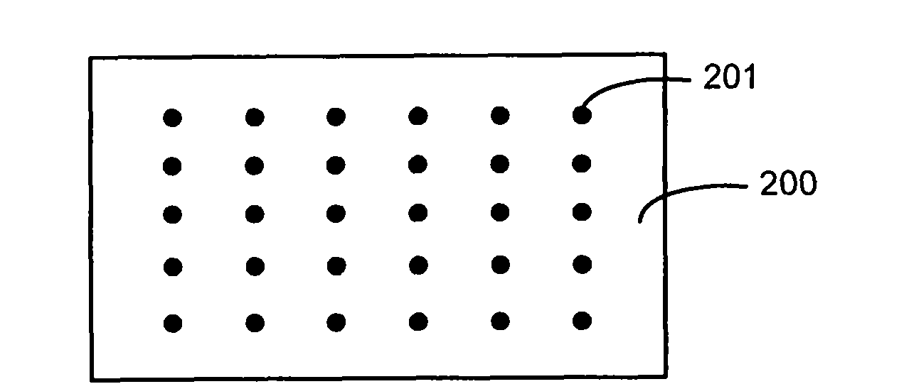
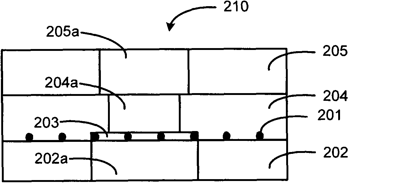

Image

  • Phase change memory element and manufacturing method thereof
  • Phase change memory element and manufacturing method thereof
  • Phase change memory element and manufacturing method thereof

Examples


Embodiment Construction

[0033] In the following description, numerous specific details are set forth in order to provide a more thorough understanding of the present invention. It will be apparent, however, to one skilled in the art that the present invention may be practiced without one or more of these details. In other instances, some technical features known in the art have not been described in order to avoid obscuring the present invention.

[0034] For a thorough understanding of the present invention, detailed steps will be presented in the following description to illustrate how the present invention can be used to fabricate phase change memory elements. Obviously, the practice of the present invention is not limited to the specific details familiar to those skilled in the semiconductor arts. Preferred embodiments of the present invention are described in detail below, however, the present invention may have other embodiments in addition to these detailed descriptions.

[0035] In order to...


PUM

PropertyMeasurementUnit
The average diameteraaaaaaaaaa
Thicknessaaaaaaaaaa

Abstract

The invention discloses a phase change memory element and a manufacturing method thereof. The phase change memory element comprises a bottom electrode, nano particles, an insulating layer, a phase change layer and a top electrode, wherein the nano particles are positioned on the upper surface of the bottom electrode; the insulating layer is formed in a region which is not covered by the nano particles on the upper surface of the bottom electrode; the phase change layer is formed on the nano particles and the insulating layer and positioned right above the bottom electrode; the top electrode is formed on the phase change layer and aligned to the bottom electrode; and the nano particles are used for electrically connecting the bottom electrode with the phase change layer. According to the phase change memory element and the manufacturing method thereof, the contact area between the bottom electrode and the phase change layer can be effectively reduced, and the heating efficiency of the bottom electrode on the phase change layer is improved, so that the read-write rate of the phase change memory element is improved.

Description

technical field [0001] The present invention relates to a semiconductor manufacturing process, in particular to a phase-change memory element and a manufacturing method thereof. Background technique [0002] Phase-change materials (such as Ge-Sb-Te phase-change materials) change their phase states into crystalline and amorphous states through local heating caused by electrical pulses. Phase-change memory elements are semiconductor devices that use this feature to store binary information. . The phase-change memory element is a resistance-based memory. The phase-change material exhibits low-resistance and high-resistance resistance characteristics through the transition between crystalline and amorphous states to achieve the purpose of storing binary information. In the phase change memory element, the memory element storing binary information includes a phase change layer and electrodes. [0003] figure 1 is a cross-sectional view of a prior art phase change memory elemen...

Claims


Application Information

Patent Timeline
IPC IPC(8): H01L45/00
Inventor 洪中山
Owner SEMICON MFG INT (SHANGHAI) CORP
Why Eureka
Try Eureka