Thin-film transistor component, pixel structure and driving circuit of display panel

A thin-film transistor and display panel technology, which is applied in the direction of transistors, circuits, electrical components, etc., can solve the problems that the frame cannot be further reduced and affects the development of narrow-frame flat display panels, etc.

Active Publication Date: 2012-03-28
AU OPTRONICS CORP
View PDF5 Cites 13 Cited by
  • Summary
  • Abstract
  • Description
  • Claims
  • Application Information

AI Technical Summary

Problems solved by technology

However, as the resolution increases, the area occupied by the GOA circuits fabricated in the peripheral area must also increase, so that the frame of the flat display panel cannot be further reduced, which affects the development of the narrow frame flat display panel.

Method used


Image

  • Thin-film transistor component, pixel structure and driving circuit of display panel
  • Thin-film transistor component, pixel structure and driving circuit of display panel
  • Thin-film transistor component, pixel structure and driving circuit of display panel

Examples


Embodiment Construction

[0029] In order to enable those of ordinary skill in the technical field of the present invention to further understand the present invention, the preferred embodiments of the present invention are listed below, together with the accompanying drawings, to describe in detail the composition of the present invention and the desired effects .

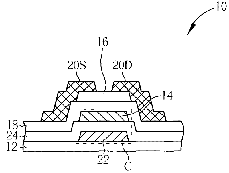
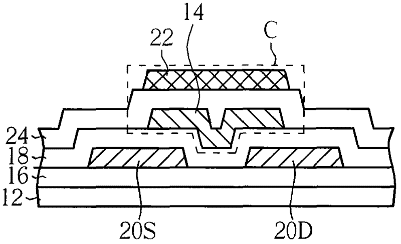
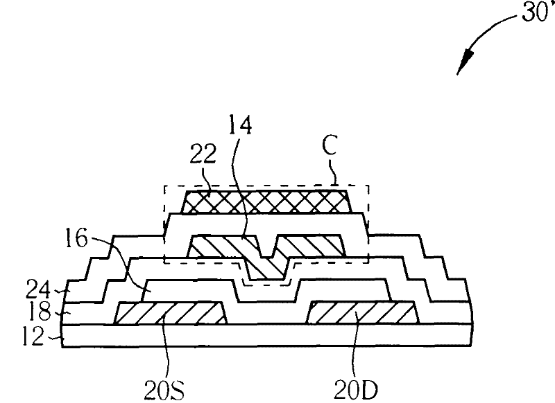
[0030] Please refer to figure 1 . figure 1 A schematic diagram of a thin film transistor device according to a first preferred embodiment of the present invention is shown. like figure 1 As shown, the thin film transistor device 10 of this embodiment is disposed on a substrate 12, such as an array substrate included in a display panel. The TFT device 10 includes a gate 14 , a semiconductor channel layer 16 , a gate insulating layer 18 , a source 20S and a drain 20D, a capacitor electrode 22 , and a capacitor dielectric layer 24 . The gate insulating layer 18 is located between the gate 14 and the semiconductor channel layer 16 , and th...


PUM


Abstract

The present invention provides a thin-film transistor component, a pixel structure and a driving circuit of a display panel. The thin-film transistor component is equipped on a substrate and comprises the following components: a grid, a semiconductor channel layer, a grid insulation layer which is provided between the grid and the semiconductor channel layer, a source and a drain which are respectively provided at two opposite sides of the semiconductor channel layer and are overlapped with the semiconductor channel layer partially, a capacitor electrode which is at least partially overlapped with the grid part, and a capacitive dielectric layer which is provided between the capacitor electrode and the grid. The capacitor electrode, the grid and the capacitive dielectric layer form a capacitor component.

Description

technical field [0001] The present invention relates to a thin film transistor element and a pixel structure and a driving circuit of a display panel, in particular to a thin film transistor element having a gate vertically overlapped with a capacitor electrode to form a capacitive element, and a display panel provided with the above thin film transistor element The pixel structure and driving circuit. Background technique [0002] Flat display panels, such as liquid crystal display panels, have replaced traditional cathode ray tube displays and become mainstream products in the display market due to their thin, light, small, low radiation, and low power consumption characteristics. In the development of flat panel display panels, narrow bezel design and high-resolution specifications are the two major development trends. In the current flat panel display panel, in order to reduce the number of driving chips, a method of integrating the gate driving circuit on the array sub...

Claims


Application Information

Patent Timeline
Patent Type & Authority Applications(China)
IPC IPC(8): H01L29/786H01L27/12G02F1/1368G09G3/36
CPCG02F1/1368H01L27/1255G09G3/36H01L29/786G09G3/3677H01L27/12G09G2310/0286G02F1/136213G02F1/136286
Inventor 张哲嘉刘圣超蔡五柳魏全生林志宏
Owner AU OPTRONICS CORP
Why Eureka
Try Eureka