Vertical Zener diode structure and preparation method thereof

A technology of Zener diodes and injection regions, which is applied in semiconductor/solid-state device manufacturing, electrical components, circuits, etc., can solve the problems of clamping circuit reliability, Zener breakdown value drift, product failure, etc., and improve product quality. Reliability, the effect of improving the drift of Zener breakdown value

Inactive Publication Date: 2012-04-11
SHANGHAI HUA HONG NEC ELECTRONICS
View PDF7 Cites 7 Cited by
  • Summary
  • Abstract
  • Description
  • Claims
  • Application Information

AI Technical Summary

Problems solved by technology

In the working state of the Zener diode with the above structure, because some carriers in the Zener breakdown will be captured by the silicon surface, the Zener breakdown value will have a relatively large drift, resulting in a reliability problem in the clamping circuit, which is serious. will cause the product to fail

Method used


Image

  • Vertical Zener diode structure and preparation method thereof
  • Vertical Zener diode structure and preparation method thereof
  • Vertical Zener diode structure and preparation method thereof

Examples


Embodiment Construction

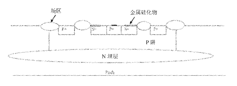
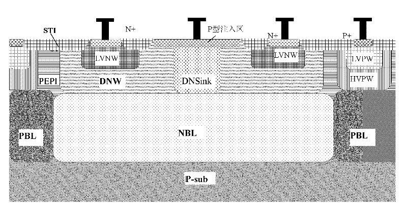
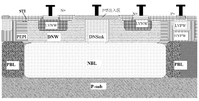
[0016] In the present invention, a vertical zener diode structure is adopted, with a built-in buried PN junction, which can improve the breakdown voltage. The vertical structure from the silicon surface to the bottom is a P-type implantation region (for shallow implantation), and the surface density is 1015 atoms. The order of magnitude per square centimeter; the N-type implantation region (for deep layer implantation), located below the P-type implantation region, has a surface density of 1014 atoms / square centimeter to 1015 atoms / square centimeter; the entire P-type implantation region and N-type implantation region are made in In an epitaxial layer with a deep N well, a dense N-type buried layer can be connected below, and the surface density is on the order of 1015 atoms / cm2. In a preferred embodiment, the vertical depth of the P-type implantation region is greater than or equal to 0.2 microns. In the vertical diode structure of the present invention, the zener breakdown p...


PUM


Abstract

The invention discloses a vertical Zener diode structure. The vertical Zener diode structure is characterized in that N-type injection areas and P-type injection areas of a Zener diode are positioned in an N trap of an epitaxial layer; and the P-type injection areas and the N-type injection areas are arranged downwards in sequence from the silicon surface in a staggered manner. The Zener breakdown point of the vertical Zener diode structure is far away from the silicon surface, so that the drift problem of the Zener breakdown value is improved. The invention also discloses a preparation method of the vertical Zener diode structure.

Description

technical field [0001] The present invention relates to a vertical Zener diode structure. The invention also relates to a preparation method of the vertical Zener diode structure. Background technique [0002] Traditional Zener diodes are formed by using a ring of N-type implants on the silicon surface surrounded by P-type implants. In the working state of the Zener diode with the above structure, because some carriers in the Zener breakdown will be captured by the silicon surface, the Zener breakdown value will have a relatively large drift, resulting in a reliability problem in the clamping circuit, which is serious. will cause the product to fail. Contents of the invention [0003] The technical problem to be solved by the present invention is to provide a vertical Zener diode device structure, which can improve the reliability of the Zener diode device. [0004] In order to solve the above-mentioned technical problems, in the vertical Zener diode structure of the pr...

Claims


Application Information

Patent Timeline
Patent Type & Authority Applications(China)
IPC IPC(8): H01L29/866H01L21/329H01L29/36
CPCH01L29/866H01L29/66106
Inventor 张帅董科
Owner SHANGHAI HUA HONG NEC ELECTRONICS
Why Eureka
Try Eureka