Shift register, display device, gate drive circuit and driving method

A technology of shift register circuit and shift register, which is applied in the direction of static memory, electrical analog memory, digital memory information, etc., which can solve the problems that are not conducive to the bonding process of module driver IC, the control signal cannot be controlled by the circuit, and the length of the driver IC increases. Large and other problems, to achieve the effect of improving voltage and drift problems, good control, and reduced drop rate

Inactive Publication Date: 2015-03-04
BOE TECH GRP CO LTD +1
View PDF6 Cites 1 Cited by
  • Summary
  • Abstract
  • Description
  • Claims
  • Application Information

AI Technical Summary

Problems solved by technology

When the resolution of small-size thin film transistor liquid crystal display is high, there are more gate and data drive outputs, and the length of the drive IC will increase, which will not be conducive to the bonding process of the module drive IC
Today, through the design of the gate drive circuit, the gate drive IC is fabricated on the glass panel through the array substrate process without increasing any process and cost in the existing manufacturing process. The basic gate drive circuit shift register unit circuit Schematic as figure 1 As shown, but the working cycle of the circuit is long, the voltage threshold has a drift problem, and the control signal cannot control the circuit well

Method used


Image

  • Shift register, display device, gate drive circuit and driving method
  • Shift register, display device, gate drive circuit and driving method
  • Shift register, display device, gate drive circuit and driving method

Examples


Embodiment 1

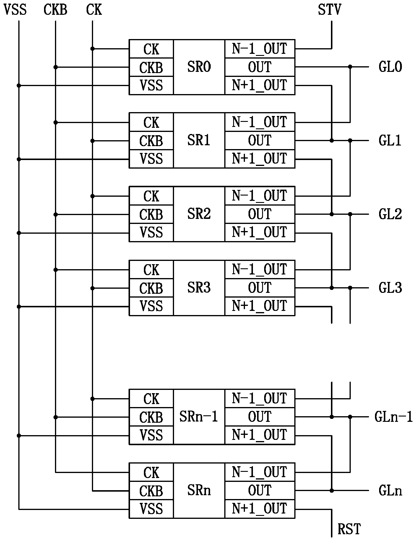
[0045] A shift register according to an embodiment of the present invention, the shift register includes a multi-stage shift register circuit such as figure 2 As shown in the figure, SR0-SRn is each stage of the n-stage shift register circuit, GL0-GLn is the output terminal of the n-stage shift register circuit, STV is the start signal, and the output of each stage of the shift register is used as the The STV start signal, the output of the lower level is used as the Reset reset signal, and it works under the double clock CK and CKB to realize the top-down gate drive scan output.

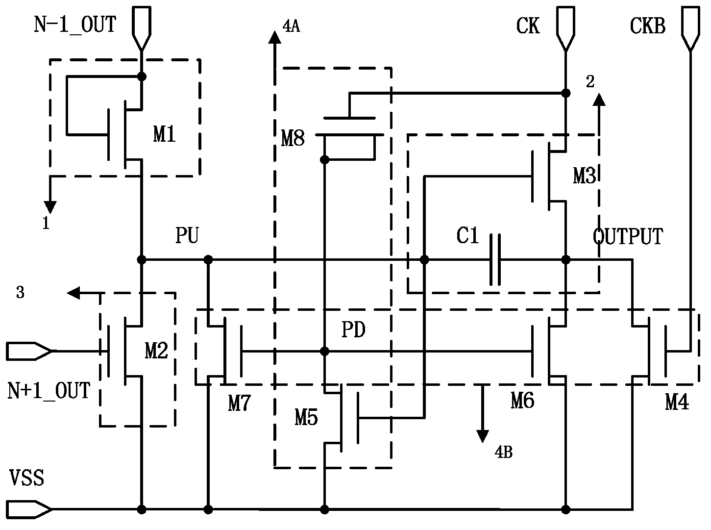
[0046] Such as image 3 As shown, the Nth stage shift register circuit of the multi-stage shift register circuit includes:

[0047] A pre-charging circuit 1 for pre-charging the pull-up circuit;

[0048] The pull-up circuit 2 is used to make the output terminal OUTPUT output a high level after the pre-charging is completed;

[0049] The reset circuit 3 resets the shift register circuit of the Nt...

Embodiment 2

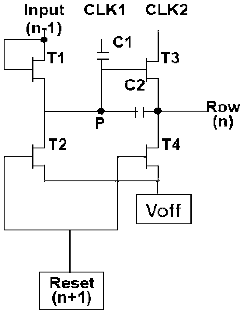
[0074] A kind of shift register of the embodiment of the present invention such as Image 6 As shown, its features are basically the same as those in Embodiment 1, except that the first holding circuit includes a fifth transistor and an eighth transistor, and the control terminal of the eighth transistor is the first control terminal of the holding circuit , the source and drain of the eighth transistor are connected to the source of the fifth transistor, the gate of the fifth transistor is connected to the control terminal of the pull-up circuit, and the drain of the fifth transistor grounding;

[0075] The second holding circuit includes a fourth transistor, a sixth transistor, and a seventh transistor, the gate of the fourth transistor is the second control terminal of the holding circuit, and the source of the fourth transistor is connected to the seventh transistor. The source is connected to the output end of the pull-up circuit, the drain of the fourth transistor is gr...


PUM


Abstract

A shift register, a display device, a gate drive circuit and a driving method. The shift register comprises a multistage shift register circuit (SR0-SRn), an Nth shift register circuit of the multistage shift register circuit comprises a precharge circuit (1), a pull-up circuit (2), a reset circuit (3) and a holding circuit, the holding circuit is provided with an eighth transistor (M8), a gate electrode of the eighth transistor (M8) is connected with a first control signal terminal (CK), and a source electrode is connected with a drain electrode. Not only is the shift registering achieved, but also a working cycle of the circuit is reduced, the voltage and the shifting problems are solved, the control of control signals to pull-down nodes is achieved through the transistor with the source electrode and the drain electrode short-circuited, the pull-down nodes are lifted rapidly when the first control signals are at a high level, the descend range of the pull-down nodes is reduced when the first control signals are at a low level, and the control of the control signals to the circuit can be achieved well.

Description

technical field [0001] The invention relates to the field of liquid crystal display, in particular to a shift register, a display device, a gate drive circuit and a drive method. Background technique [0002] In TFT-LCD, the basic principle of realizing a frame display is to output the signal required by each row of pixels from top to bottom through data drive, and gate drive to each pixel row from top to bottom in turn. Input a square wave with a certain width for gating. The current manufacturing method is to bond the gate driver IC and data driver IC on the glass panel through the COG (chip on glass) process. When the resolution of the small-size thin film transistor liquid crystal display is high, the gate and data drive outputs are more, and the length of the driver IC will increase, which will not be conducive to the bonding process of the module driver IC. Today, through the design of the gate drive circuit, the gate drive IC is fabricated on the glass panel through...

Claims


Application Information

Patent Timeline
Patent Type & Authority Patents(China)
IPC IPC(8): G09G3/36G11C19/28
CPCG11C19/28G09G2310/0286G09G3/3677G09G2300/0408G11C19/287G09G3/3611H03K17/302G11C27/04
Inventor 吴博祁小敬周全国聂磊森
Owner BOE TECH GRP CO LTD
Why Eureka
Try Eureka