
Apparatus and system for cleaning substrate

A substrate and cleaning technology, applied in the direction of cleaning methods and appliances, chemical instruments and methods, electrical components, etc., can solve problems such as difficulties

Inactive Publication Date: 2012-04-18
LAM RES CORP
View PDF6 Cites 2 Cited by
  • Summary
  • Abstract
  • Description
  • Claims
  • Application Information

AI Technical Summary

Problems solved by technology

It is quite difficult to remove such small particle contamination without adversely affecting the features on the wafer

Method used


Image

  • Apparatus and system for cleaning substrate
  • Apparatus and system for cleaning substrate
  • Apparatus and system for cleaning substrate

Examples


Embodiment Construction

[0016] In the following description, numerous specific details are set forth in order to provide a thorough understanding of the present invention. It will be apparent, however, to one skilled in the art that the present invention may be practiced without some or all of these specific details. In other instances, well known process operations have not been described in detail in order not to unnecessarily obscure the present invention.

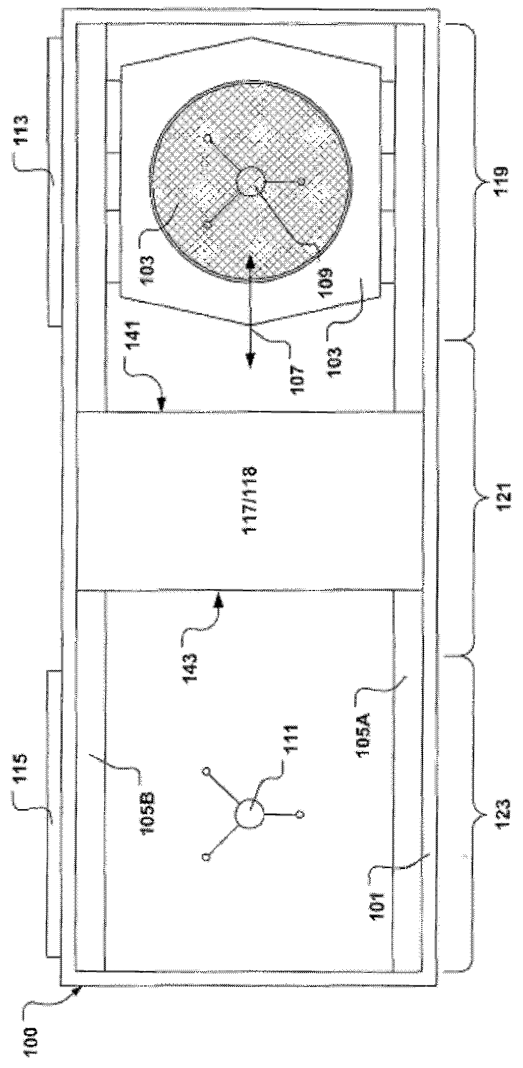
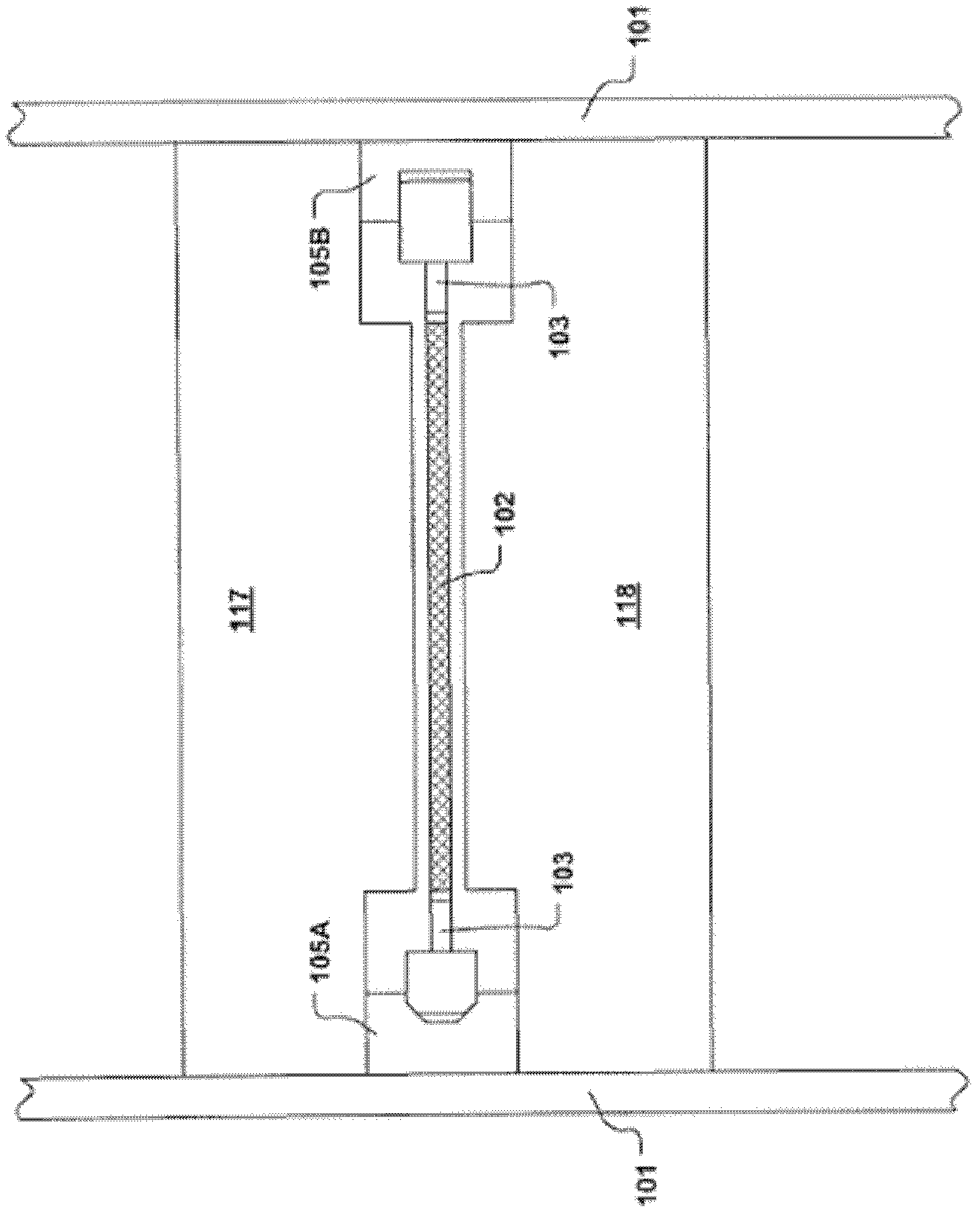
[0017] Substrates referred to herein mean, but are not limited to, semiconductor wafers, hard drive disks, optical disks, glass substrates, flat panel display surfaces, and liquid crystal display surfaces, etc., which may be contaminated during manufacturing or processing operations. Depending on the actual substrate, surfaces can be contaminated in different ways, and acceptable levels of contamination are defined in the particular industry in which the substrate is processed. For ease of discussion, substrate contamination is described here...


PUM


Abstract

An upper processing head includes a topside module defined to apply a cleaning material to a top surface of a substrate and then expose the substrate to a topside rinsing meniscus. The topside module is defined to flow a rinsing material through the topside rinsing meniscus in a substantially uni-directional manner towards the cleaning material and opposite a direction of movement of the substrate. A lower processing head includes a bottomside module defined to apply a bottomside rinsing meniscus to the substrate so as to balance a force applied to the substrate by the topside rinsing meniscus. The bottomside module is defined to provide a drain channel for collecting and draining the cleaning material dispensed from the upper processing head when the substrate is not present between the upper and lower processing heads.; The upper and lower processing heads can include multiple instantiations of the topside and bottomside modules, respectively.

Description

Background technique [0001] In the fabrication of semiconductor devices, such as integrated circuits and memory cells, a series of fabrication operations are performed to define the characteristics of a semiconductor wafer ("wafer"). A wafer (or substrate) includes integrated circuit devices in the form of a multi-level structure defined on a silicon substrate. At the substrate level, transistor devices with diffusion regions are formed. At subsequent levels, interconnect metal lines are patterned and electrically connected to transistor devices to define the desired integrated circuit device. In addition, the patterned conductive layer is insulated from other conductive layers by a dielectric material. [0002] During a series of manufacturing operations, wafer surfaces are exposed to various types of contaminants. Anything present in a manufacturing operation is by its nature a potential source of contamination. For example, sources of contamination may include process g...

Claims


Application Information

Patent Timeline
IPC IPC(8): H01L21/302H01L21/304
CPCH01L21/67051Y10S134/902H01L21/302
Inventor 林成渝(肖恩)马克·卡瓦古奇马克·威尔考克森拉塞尔·马丁利昂·金兹伯格
Owner LAM RES CORP
Features
  • Generate Ideas
  • Intellectual Property
  • Life Sciences
  • Materials
  • Tech Scout
  • Unparalleled Data Quality
  • Higher Quality Content
  • 60% Fewer Hallucinations
Learn More