Hybrid stacked structure composed of photo diode and capacitive secondary base
A photosensitive diode and capacitive technology, applied in the direction of circuits, electrical components, semiconductor devices, etc., can solve problems such as improper operation, increased substrate size, and one-time positioning error, so as to improve accuracy and production speed, reduce costs and The effect of heavy industry and loose interior space
- Summary
- Abstract
- Description
- Claims
- Application Information
AI Technical Summary
Problems solved by technology
Method used
Image

Examples
Embodiment Construction
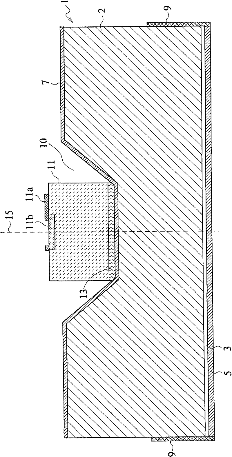
[0078] figure 1 A schematic cross-sectional view of a hybrid stack structure composed of a photodiode and a capacitive submount according to an embodiment of the invention is shown. Such as figure 1 As shown, the hybrid stack structure includes a capacitive submount 1 . The capacitive submount 1 may include: a silicon substrate 2 with a groove 10 formed on its upper surface; a dielectric layer 3 formed on the lower surface of the silicon substrate 2; a first electrode 5 deposited on the dielectric layer 3; The second electrode 7 is deposited on the upper surface of the silicon substrate 2 and the surface of the groove 10 . The photodiode 11 can include an upper electrode 11 a , a PN junction 11 b , and a lower electrode 13 , and the bottom of the groove 10 has a size that can match the size of the photodiode 11 . The photodiode 11 can be electrically bonded on the second electrode 7 at the bottom of the groove 10 through a conductive layer (not shown), and aligned with th...
PUM
 Abstract
Description
Claims
Application Information
 - R&D Engineer
- R&D Manager
- IP Professional
- Industry Leading Data Capabilities
- Powerful AI technology
- Patent DNA Extraction
Browse by: Latest US Patents, China's latest patents, Technical Efficacy Thesaurus, Application Domain, Technology Topic.
© 2024 PatSnap. All rights reserved.Legal|Privacy policy|Modern Slavery Act Transparency Statement|Sitemap