

Compression molding method and compression mold for semiconductor chip
A compression molding, semiconductor technology, applied in the direction of semiconductor devices, semiconductor/solid-state device manufacturing, semiconductor/solid-state device components, etc., can solve the problems of inability to efficiently improve product productivity, longer resin material supply time, and increased production costs.
- Summary
- Abstract
- Description
- Claims
- Application Information
AI Technical Summary
Problems solved by technology
Method used
Image

Examples
Embodiment 1
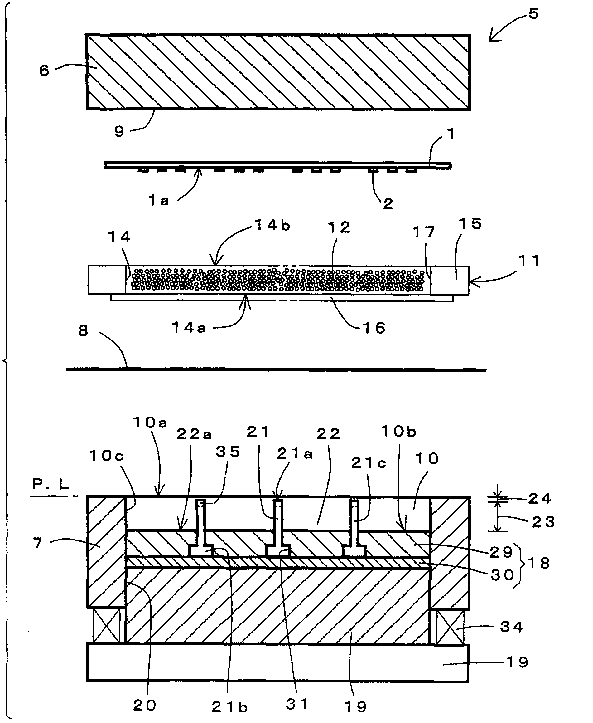
[0041] First, use Figure 1~Figure 9 and Figure 13A Example 1 will be described in detail. figure 1 , figure 2 , image 3 ,Figure 4, Figure 5 , Figure 7 and Figure 8 This is the mold for compression molding of the semiconductor chip of Example 1. Image 6 It is a cavity bottom surface member set in the mold of Example 1, and a partition member that is detachably installed on the cavity bottom surface member. Picture 9 It is a partition member installed on the bottom surface member of the cavity, and the bottom surface member of the cavity is installed on the mold of Example 1. Figure 13A This is the molded substrate of Example 1.
[0042] Regarding the substrate used in this embodiment
[0043] On the substrate 1 used in the present embodiment, semiconductor chips 2 such as IC (Integrated Circuit) are mounted in a matrix-type configuration as necessary. In addition, in this embodiment, the molded substrate 4 can be formed by sealing the semiconductor chips 2 mounted in a mat...
Embodiment 2
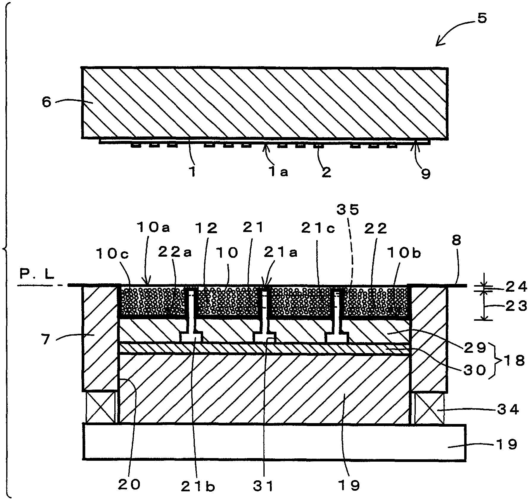
[0092] Next, use Picture 10 , Figure 11A~Figure 11C , Figure 13B Example 2 will be described in detail.
[0093] Picture 10 , Figure 11A~Figure 11C This is the mold for compression molding of the semiconductor chip of Example 2. Figure 13B It is a molded substrate molded using the mold shown in Example 2. In addition, since the basic structure of the mold shown in Example 2 is the same as that of the mold shown in Example 1, a detailed description thereof will not be repeated. In addition, the substrate used in Example 2 is the same as the substrate used in Example 1. In addition, the mold of Example 2 is provided with sprues on both sides of the partition member in the lower cavity.
[0094] About the structure of the mold for compression molding of semiconductor chips of Example 2
[0095] in Picture 10 and Figure 11A~Figure 11C In the shown mold 41, the upper mold 42 and the lower mold 43 are provided in the same manner as in Example 1. In addition, the mold 41 include...
Embodiment 3
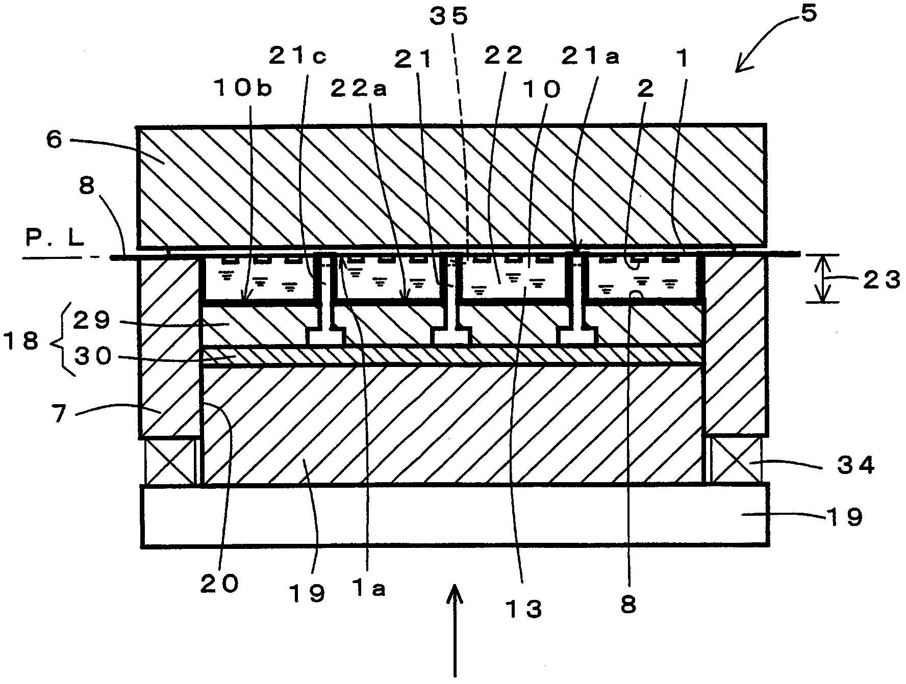
[0114] Next, use Figure 12A~Figure 12B Example 3 will be described in detail. Figure 12A~Figure 12B It is the main part of another mold for compression molding of semiconductor chips, and a partition member is detachably provided on the cavity bottom member. In addition, since the basic structure of the mold shown in Example 3 is the same as that of the mold shown in Example 1, the detailed description thereof will not be repeated. In addition, the substrate used in Example 3 is the same as the substrate used in Example 1.
[0115] About the structure of the mold for compression molding of semiconductor chips of Example 3
[0116] The basic structure of the mold shown in Example 3 is the same as that of the mold shown in Example 1. in Figure 12A~Figure 12B In the shown mold, the cavity bottom surface member 141 and the partition member 142 are provided in the same manner as in Example 1. It is provided so that the partition member 142 can be attached to the cavity bottom surf...
PUM
| Property | Measurement | Unit |
|---|---|---|
| thickness | aaaaa | aaaaa |
Abstract
Description
Claims
Application Information