
Light-emitting diode packaging structure

A technology of light-emitting diodes and packaging structures, which is applied in the direction of electrical components, circuits, semiconductor devices, etc., and can solve the problem that the position of the welding pad cannot be adjusted.

Inactive Publication Date: 2014-10-15
ZHANJING TECH SHENZHEN +1
View PDF4 Cites 0 Cited by
  • Summary
  • Abstract
  • Description
  • Claims
  • Application Information

AI Technical Summary

Problems solved by technology

[0002] Usually, the welding pads of the LED packaging structure are electroplated on the substrate, and the welding pads cannot slide relative to the substrate. After the LED packaging structure is manufactured, the position of the welding pads cannot be adjusted.

Method used


Image

  • Light-emitting diode packaging structure
  • Light-emitting diode packaging structure
  • Light-emitting diode packaging structure

Examples


Embodiment Construction

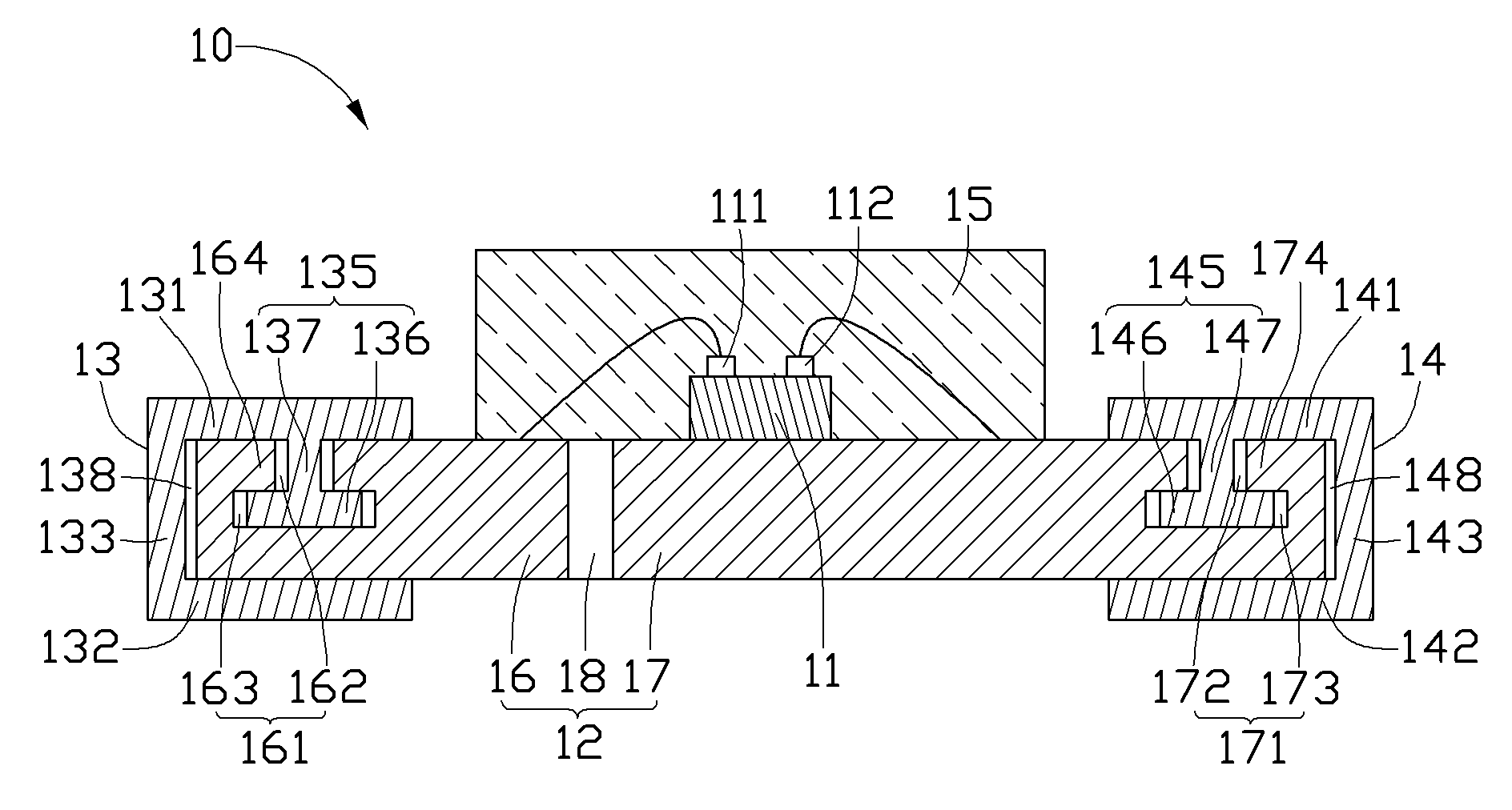
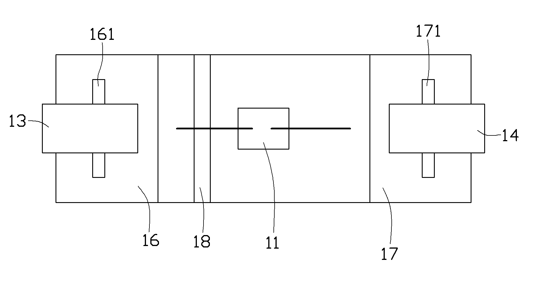
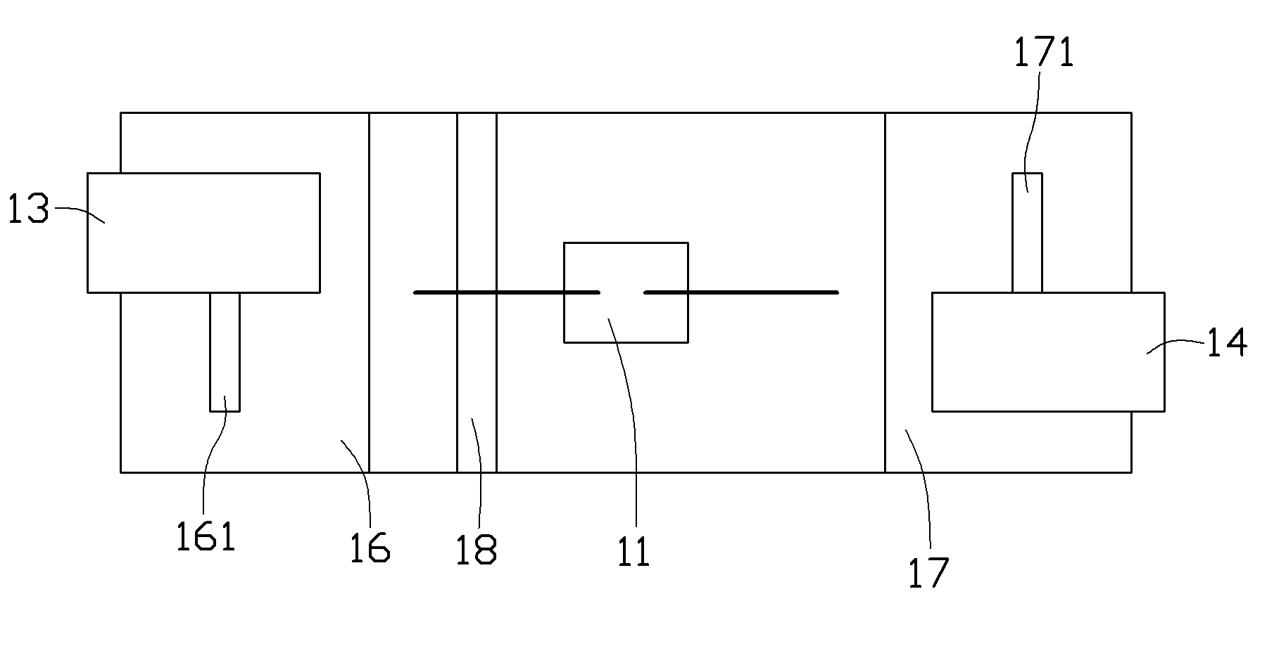
[0044] see figure 1 and figure 2 A light emitting diode packaging structure 10 provided in an embodiment of the present invention includes a light emitting diode die 11 , a conductive substrate 12 , a first pad 13 , a second pad 14 and a package body 15 .

[0045] The conductive substrate 12 includes a first conductive region 16 and a second conductive region 17 which are insulated from each other, and the first conductive region 16 and the second conductive region 17 are connected by an insulating material 18 . The first conductive area 16 defines a first sliding slot 161 , the second conductive area 17 defines a second sliding slot 171 , and the first sliding slot 161 and the second sliding slot 171 are parallel to each other. The first chute 161 is narrow on the outside and wide on the inside. The first chute 161 includes a first horizontal section 163 and a first vertical section 162 . The intersection of the straight segments 162 forms a first shoulder 164 . The secon...


PUM


Abstract

The invention relates to an LED (Light Emitting Diode) packaging structure, which comprises LED crystal grains, a conductive substrate, a first welding pad and a second welding pad. The conductive substrate comprises a first conductive region and a second conductive region which are mutually insulated, the LED crystal grains are fixed on the conductive substrate, the first conductive region is provided with a first sliding slot, the second conductive region is provided with a second sliding slot, the first welding pad comprises a first buckling part, the second welding pad comprises a second buckling part, the first buckling part is contained in the first sliding slot in a sliding manner, the first welding pad is in contact with the first conductive region, the second welding pad comprises a second buckling part, the second buckling part is contained in the second sliding slot in a sliding manner, and the second welding pad is in contact with the second conductive region. The first welding pad and the second welding pad of the LED packaging structure can respectively slide corresponding to the conductive substrate, thus the welding position of a circuit board can be matched by regulating the positions of the first welding pad and the second welding pad when the LED packaging structure is arranged on the circuit board.

Description

technical field [0001] The invention relates to a semiconductor light-emitting element, in particular to a light-emitting diode packaging structure. Background technique [0002] Usually, the welding pads of the light emitting diode packaging structure are electroplated on the substrate, and the welding pads cannot slide relative to the substrate. After the light emitting diode packaging structure is manufactured, the positions of the welding pads cannot be adjusted. Contents of the invention [0003] In view of this, it is necessary to provide a light emitting diode packaging structure that can adjust the position of the welding pad. [0004] A light-emitting diode packaging structure, including a light-emitting diode crystal grain, a conductive substrate, a first welding pad, and a second welding pad, the conductive substrate includes a first conductive region and a second conductive region that are insulated from each other, and the light-emitting diode crystal grain is...

Claims


Application Information

Patent Timeline
Patent Type & Authority Patents(China)
IPC IPC(8): H01L33/48H01L33/62
Inventor 罗杏芬柯志勋詹勋伟
Owner ZHANJING TECH SHENZHEN
Learn More