

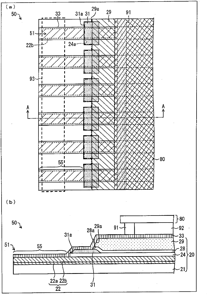
Wiring board, method for manufacturing same, display panel and display device
一种配线基板、制造方法的技术,应用在辨认装置、照明装置、半导体/固态器件制造等方向,能够解决金属配线腐蚀等问题,达到防止腐蚀和断线、促进侵入的效果
- Summary
- Abstract
- Description
- Claims
- Application Information
AI Technical Summary
Problems solved by technology
Method used
Image

Examples
Embodiment approach 1
[0069] Mainly based on figure 1 (a), (b) and Figure 7 (a)~(c), Figure 19 with Figure 20 One embodiment of the present invention will be described below.
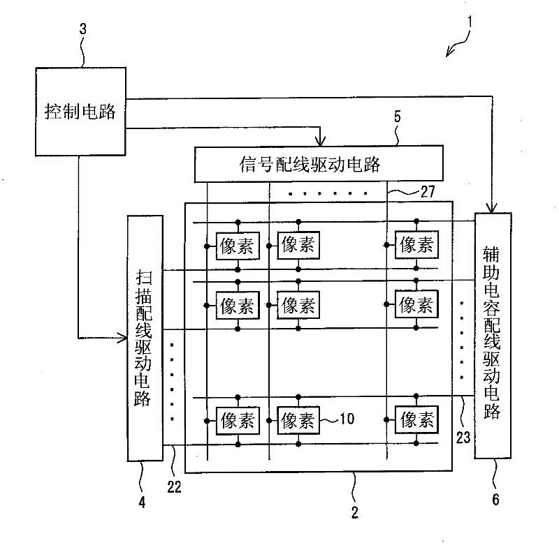
[0070] figure 2 It is a block diagram showing a schematic configuration of main parts of the liquid crystal display device of the present embodiment.
[0071] Such as figure 2 As shown, the liquid crystal display device 1 of the present embodiment includes: a liquid crystal panel 2 (display panel) in which pixels 10 are arranged in a matrix; a driving circuit for driving the liquid crystal panel 2; and a control circuit 3 for controlling the driving of the driving circuit. A backlight unit (not shown) etc. are provided as needed.
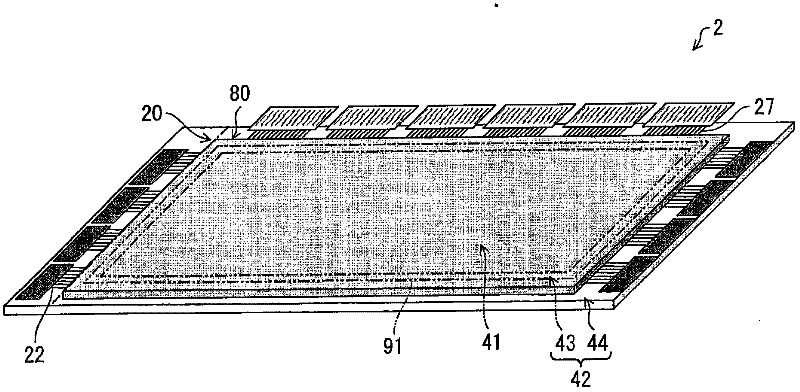
[0072] The liquid crystal panel 2 is provided with a plurality of scanning lines 22 and a plurality of signal lines 27 respectively crossing the respective scanning lines 22 , and pixels 10 are provided for each combination of these scanning lines 22 and signal lines 27 . (pixel part)...
Embodiment approach 2
[0245] based on Figure 8 Other embodiments of the present invention will be described below. In addition, in this embodiment, differences from the above-mentioned first embodiment will be mainly described, and components having the same functions as those in the above-mentioned first embodiment will be given the same reference numerals, and description will be omitted.
[0246]Also in this embodiment, similarly to the above-mentioned first embodiment, the scanning line connection portion 50 is illustrated as the connection portion 44, but the scanning line connection portion 50, the scanning line 22, the scanning terminal 51, and the scanning electrode 12 can be connected to each other. Rename them to the signal wire connection part 60, the connection wire 62, the signal terminal 61, and the signal electrode 13, respectively. In addition, the names of the metal layers (wirings) can be changed in the same way as in the storage capacitor wiring connections.
[0247] Figure ...
Embodiment approach 3
[0254] based on Figure 9 (a), (b) The other embodiment of this invention is demonstrated as follows. In addition, in this embodiment, differences from the above-mentioned first embodiment will be mainly described, and components having the same functions as those in the above-mentioned first embodiment will be given the same reference numerals, and descriptions thereof will be omitted.
[0255] In addition, in this embodiment, similarly to Embodiments 1 and 2, the scanning line connection portion 50 is described as the connection portion 44 as an example, but the scanning line connection portion 50 , the scanning line 22 , the scanning terminal 51 , and the scanning electrode 12 They can be renamed as the signal wire connection part 60, the connection wire 62, the signal terminal 61, and the signal electrode 13, respectively. In addition, the names of the metal layers (wirings) can be changed in the same way as in the storage capacitor wiring connections.
[0256] Figure ...
PUM
 Abstract
Description
Claims
Application Information