Aluminum pore-filling connection process

A connection and process technology, applied in the field of semiconductor manufacturing process, can solve the problems of low film forming rate, easy formation of voids in aluminum filling holes, affecting the throughput of film forming equipment, etc., and achieve the effect of reducing the impact of throughput and lowering requirements

Active Publication Date: 2014-02-26
SHANGHAI HUAHONG GRACE SEMICON MFG CORP
View PDF4 Cites 0 Cited by
  • Summary
  • Abstract
  • Description
  • Claims
  • Application Information

AI Technical Summary

Problems solved by technology

like figure 1 As shown, when the upper half of the wall of the hole 12 to be filled on the silicon wafer is an oxide film (silicon dioxide) 11 and the opening is small, and the lower half is silicon 10 and the hole is larger, for such a hole, if The conventional aluminum filling and wiring process is used to directly deposit an aluminum film on the silicon wafer to fill the hole. Aluminum filling is easy to form voids. In order to prevent the formation of voids, it is generally used to reduce the deposition power (such as 1200W) and increase the deposition temperature (such as 480W). Celsius) method to fill the holes, but this will make the film forming rate lower, affect the throughput of the film forming equipment, and also require the aluminum film forming equipment to have a higher temperature control heating capacity

Method used


Image

  • Aluminum pore-filling connection process
  • Aluminum pore-filling connection process
  • Aluminum pore-filling connection process

Examples


Embodiment Construction

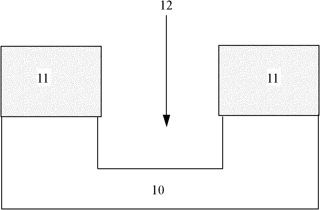
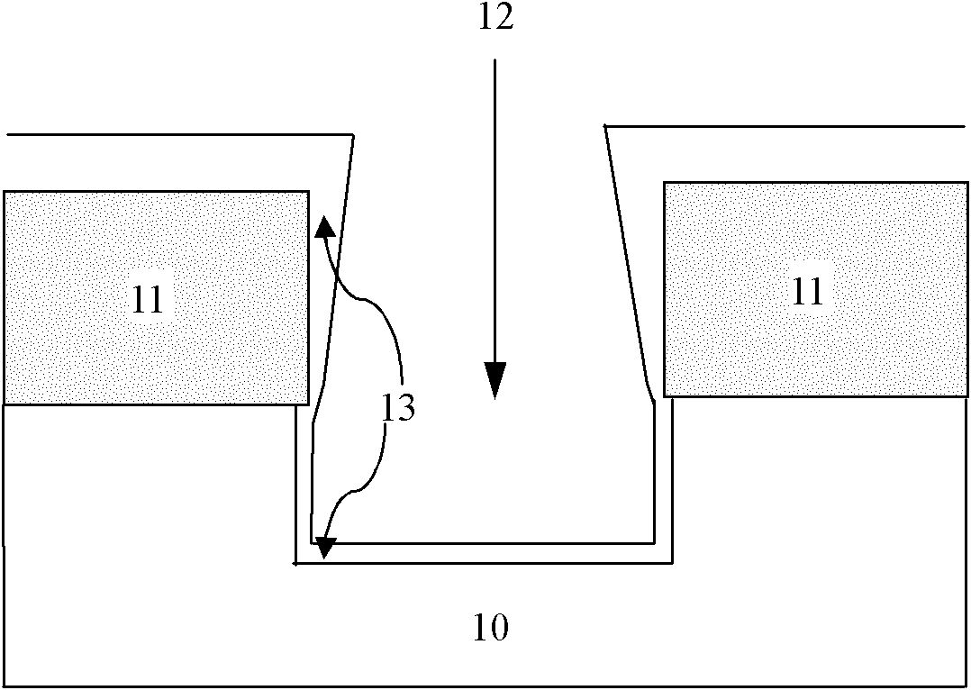
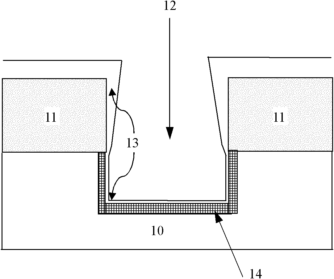
[0019] An embodiment of the aluminum filling hole connection process of the present invention is as follows: Figure 2 ~ Figure 4 shown, including the following steps:

[0020] 1. Deposit a layer of metal (titanium) on the silicon wafer, such as figure 2 As shown, a layer of metal (titanium) 13 is deposited on the oxide film (silicon dioxide) 11 on the silicon wafer and the surface of the silicon 10;

[0021] 2. The metal (titanium) 13 deposited on the silicon wafer reacts with silicon 10 to form an alloy (titanium-silicon alloy) 14 by means of thermal annealing, such as image 3 Shown; The top half of the wall of the hole 12 that needs to be filled on the silicon chip is that the oxide film will not react with the metal (titanium) 13 deposited on the silicon chip, so the volume does not change, and the hole 12 that needs to be filled on the silicon chip Because the lower half of the wall is made of silicon, it will react with the metal (titanium) 13 deposited on the silico...


PUM

PropertyMeasurementUnit
thicknessaaaaaaaaaa

Abstract

The invention discloses an aluminum pore-filling connection process, which includes the steps: firstly, depositing a metal layer on a silicon slice; secondly, reacting metal deposited on the silicon slice with silicon by means of thermal annealing to form an alloy; thirdly, etching metal unreacted with the silicon by the aid of liquid chemicals through wet treatment; and fourthly, depositing an aluminum film to form an aluminum connection by means of etching. By the aid of the aluminum pore-filling connection process, aluminum film forming equipment is capable of depositing the aluminum film on the silicon slice to realize aluminum pore-filling at a common film forming temperature and a common film forming power, and cavities are not easy to form during aluminum pore-filling.

Description

technical field [0001] The invention relates to a semiconductor manufacturing process, in particular to an aluminum filling hole connection process. Background technique [0002] Aluminum is the back-end process of integrated circuit manufacturing. In the semiconductor manufacturing process, the aluminum filling and wiring process is a relatively mature technology with its stable process, relatively low cost performance and mature technology. a wide range of applications. Aluminum wiring can be used as a flat wiring to connect the gap, or directly as a filling material to replace the traditional tungsten plug. [0003] The conventional aluminum filling and wiring process is to directly deposit an aluminum film on a silicon wafer, and then use an etching method to form an aluminum wiring. Such as figure 1 As shown, when the upper half of the wall of the hole 12 to be filled on the silicon wafer is an oxide film (silicon dioxide) 11 and the opening is small, and the lower h...

Claims


Application Information

Patent Timeline
Patent Type & Authority Patents(China)
IPC IPC(8): H01L21/768H01L21/24
Inventor 季芝慧李晓远
Owner SHANGHAI HUAHONG GRACE SEMICON MFG CORP
Why Eureka
Try Eureka