
Liquid crystal display device

A liquid crystal display device and electrode technology, applied in nonlinear optics, instruments, optics, etc., can solve the problems of different deflection directions, reduce the actual transmittance of pixels, etc., and achieve the effect of improving response time and transmittance

Active Publication Date: 2015-02-18
KUSN INFOVISION OPTOELECTRONICS
View PDF5 Cites 0 Cited by
  • Summary
  • Abstract
  • Description
  • Claims
  • Application Information

AI Technical Summary

Problems solved by technology

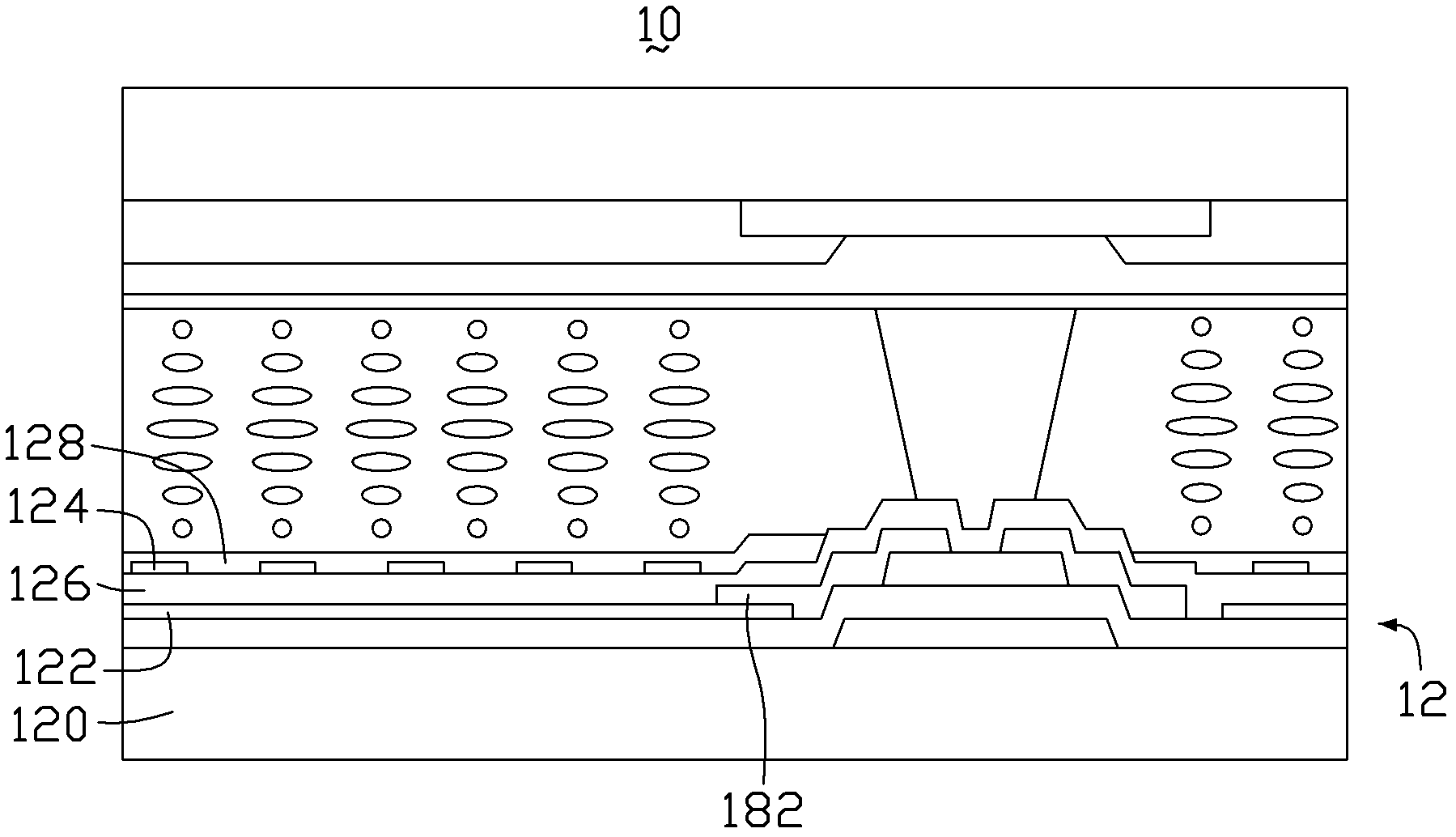
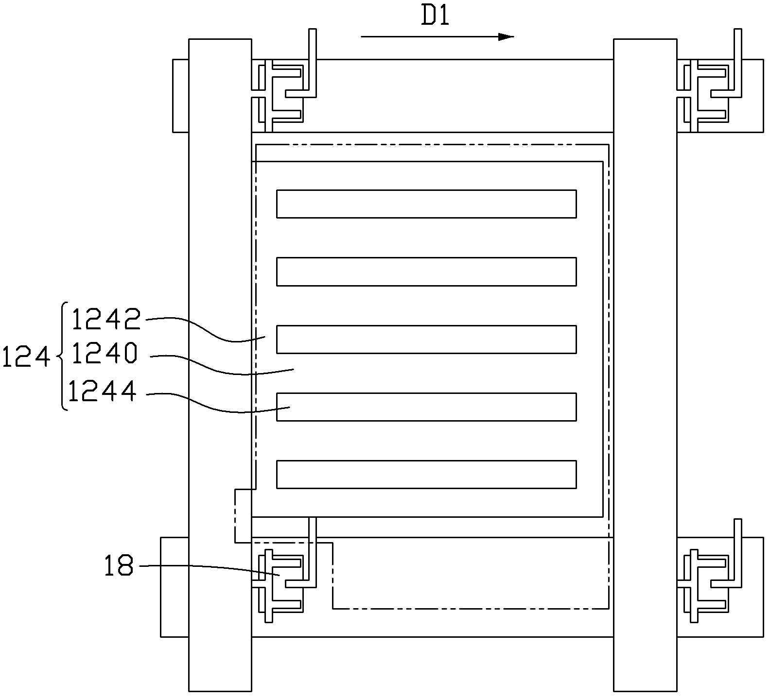
[0005] However, in the existing FFS liquid crystal display device 10, in the region where the two strip-shaped vertical conductive portions 1242 of the common electrode 124 are located, since the two strip-shaped vertical conductive portions 1242 in the common electrode 124 are connected to the The electric field generated between the pixel electrodes 122 is distributed along both sides of the vertical conductive portion 1242, and in the area between the two vertical conductive portions 1242, the plurality of strip-shaped horizontal conductive portions 1240 in the common electrode 124 are connected to the pixel electrode 122 The electric field generated between them is distributed along both sides of the horizontal conductive portion 1240. Therefore, in the liquid crystal layer of the liquid crystal display device 10, in the area corresponding to the two vertical conductive portions 1242 in the common electrode 124, the liquid crystal molecules are respectively subjected to two different directions. Therefore, after the external driving voltage is applied, the liquid crystal molecules in these two regions will be affected by the electric fields in two different directions, so that the phenomenon of disclination (Disclination line) will appear, that is, the liquid crystal molecules in this region will appear. Different deflection directions, or even basically no rotation, cause the area to always appear in a dark state, reducing the actual transmittance of the pixel

Method used


Image

  • Liquid crystal display device
  • Liquid crystal display device
  • Liquid crystal display device

Examples


Embodiment Construction

[0030] In order to further explain the technical means and effects of the present invention to achieve the intended purpose of the invention, the specific implementation methods, methods, steps, structures, and features of the liquid crystal display device proposed according to the present invention will be described below in conjunction with the accompanying drawings and preferred embodiments. And effect, detailed description is as follows.

[0031] The aforementioned and other technical contents, features and effects of the present invention will be clearly presented in the following detailed description of the preferred embodiments with reference to the drawings. Through the description of specific implementation methods, the technical means and effects of the present invention to achieve the intended purpose can be understood more deeply and specifically, but the attached drawings are only for reference and description, and are not used to explain the present invention lim...


PUM


Abstract

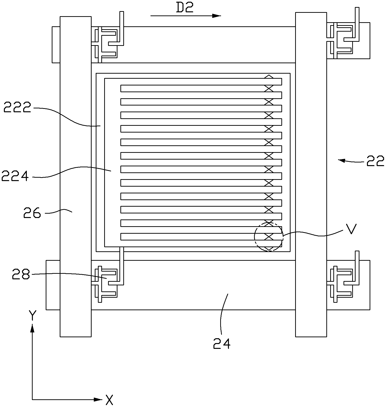
The invention provides a liquid crystal display device. A first electrode and a second electrode are arranged in a pixel area. The second electrode comprises a plurality of first strip-type conductive parts and a second strip-type conductive part. Each of the plurality of first conductive parts has a first terminal and a second terminal which are opposite to each other. The first terminals of the plurality of first conductive parts are connected together through the second conductive part, and the second terminals of the plurality of first conductive parts are disconnected from one another. Openings are reserved in areas between every two adjacent first conductive parts and close to the second terminals in the first electrode, and electrode bumps are formed by the openings. When the liquid crystal display device works, component electric fields in a direction vertical to the first conductive parts are formed between the electrode bumps of the first electrode and the second electrode. Compared with the prior art, the liquid crystal display device has high light transmittance and quick response.

Description

technical field [0001] The invention relates to the field of photoelectric display technology, and in particular to a liquid crystal display device. Background technique [0002] At present, as a kind of flat panel display, a liquid crystal display device has been widely used in various fields because of its advantages of low power consumption, thin shape and light weight. Generally, a liquid crystal panel in a liquid crystal display device includes a thin film transistor array substrate, a color filter substrate, and a liquid crystal layer filled between the thin film transistor array substrate and the color filter substrate. The thin film transistor array substrate includes a plurality of gate lines, a plurality of data lines, a plurality of pixel areas defined by the cross arrangement of the plurality of gate lines and the plurality of data lines, and the like. The pixel area includes a pixel electrode, a common electrode, and a thin film transistor (Thin Film Transistor...

Claims


Application Information

Patent Timeline
Patent Type & Authority Patents(China)
IPC IPC(8): G02F1/1343G02F1/1362G02F1/1368
Inventor 钟德镇邱郁雯李永谦黄霞
Owner KUSN INFOVISION OPTOELECTRONICS
Learn More