Method for packaging LED illuminating device

A technology of LED lighting and packaging methods, which is applied in the direction of electrical components, circuits, semiconductor devices, etc., can solve the problems of LED lighting devices such as large volume, excessive glare, complex structure, etc., and achieve the advantages of reducing heat conduction process, beautiful appearance, and simple packaging process Effect

Inactive Publication Date: 2013-09-18
HANGZHOU DIANZI UNIV
View PDF2 Cites 0 Cited by
  • Summary
  • Abstract
  • Description
  • Claims
  • Application Information

AI Technical Summary

Problems solved by technology

[0004] The purpose of the present invention is to overcome the shortcomings of the traditional LED packaging method, such as large volume, difficult heat dissipation, high cost, excessive glare, etc. Problems such as cumbersome process and uneven chromaticity

Method used


Image

  • Method for packaging LED illuminating device
  • Method for packaging LED illuminating device
  • Method for packaging LED illuminating device

Examples


Embodiment 1

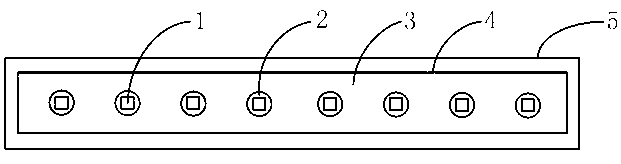
[0037] Such as image 3 As shown, it is a structural schematic diagram of a strip-shaped LED lighting device realized by the packaging method of the present invention.

[0038] The substrate 5 is made of a material with high thermal conductivity; the LED chip 1 is bonded with silver glue and fixed on the crystal-bonding position on the substrate 5 with the coating 2; the silica gel 4 is coffered on the substrate 5; the packaging material 3 is coated on The substrate 5 completely covers the LED chips 1 and is bonded to the substrate 5 .

[0039] Among them, the packaging material 3 is made of fluorescent powder mixed with glue, which has good fluidity, high refractive index, and high temperature resistance. The coffered silica gel 4 ensures the stability of its shape and position, and the formed fluorescent glue layer is flat. , the thickness is uniform and uniform, and no other medium is produced between the LED chip 1 and the interface loss of light is reduced.

Embodiment 2

[0041] Such as Figure 4 As shown, it is a structural schematic diagram of a circular LED lighting device realized by the packaging method of the present invention.

[0042] It is roughly the same as Embodiment 1, except that the circuit wiring on the substrate 5 is different, the shape of the substrate 5 is circular, the shape of the cofferdam of the silica gel 4 is also circular, and the packaging method is completely the same.

[0043] The above-mentioned embodiment 1 and embodiment 2 realize the integrated packaging of multiple LED chips on one circuit board, reduce the secondary optical lens to one, and cooperate with the mirror-like coating to enhance reflection and improve light extraction efficiency; no need for single-point glue point by point , with a higher yield.


PUM


Abstract

The invention relates to a method for packaging an LED illuminating device. Traditional LED packaging methods have the defects of difficulty in heat dissipation, large size of the LED illuminating device and the like. The method includes: coating, namely coating a metal layer on a die bonding position of a substrate with wires well distributed; die bonding, namely using silver paste to fix an LED chip onto the die bonding position of the substrate; lead bonding, namely using gold wire to electrically connect the LED chip with the substrate; silicone enclosing, namely coating silicone on the substrate to form a hollow polygon; infusing packaging materials, namely drip infusing the packaging materials in an area enclosed by the silicone to cover the LED chip; and curing, namely baking the whole substrate to lead the packaging materials to be fixedly molded to obtain the LED illuminating device. The LED chip is directly packaged on the substrate by means of die bonding and the on-substrate chip packaging technique, so that heat conduction is reduced, thermal resistance of the LED chip is reduced, heat dissipating performance of the LED illuminating device can be improved while dimension of the LED illuminating device is reduced, and the service life of the LED illuminating device is prolonged.

Description

technical field [0001] The invention belongs to the technical field of LED packaging, and in particular relates to a packaging method of an LED lighting device. Background technique [0002] The traditional LED packaging method is to package the LED chip and bracket into an independent device, after slotting, patching, wire bonding, dispensing, and then baking to form a patch LED, which is then soldered to the substrate when used. Such a packaging method requires all the steps of packaging each LED chip separately. The production cycle is long and the process is complicated. Moreover, the thermal channel of the packaging structure formed by this method is long, which makes the junction temperature of the LED rise, which leads to overheating of the LED chip and low light output. Reduce and shorten the service life. When applied to lighting devices, there are still problems such as large volume, many particles, excessive glare, and high cost, which are not conducive to the de...

Claims


Application Information

Patent Timeline
Patent Type & Authority Patents(China)
IPC IPC(8): H01L33/00
Inventor 秦会斌祁姝琪丁申冬郑梁邵李焕
Owner HANGZHOU DIANZI UNIV
Why Eureka
Try Eureka