Method for detecting line insulation of circuit board
A circuit board circuit and circuit board technology, applied in the direction of measuring electrical variables, measuring resistance/reactance/impedance, measuring devices, etc., can solve problems such as misjudgment, inaccurate test data, and test data deviation from standard data, etc., to eliminate errors , High common mode rejection capability, low zero drift effect
- Summary
- Abstract
- Description
- Claims
- Application Information
AI Technical Summary
Problems solved by technology
Method used
Image
Examples
Embodiment 1
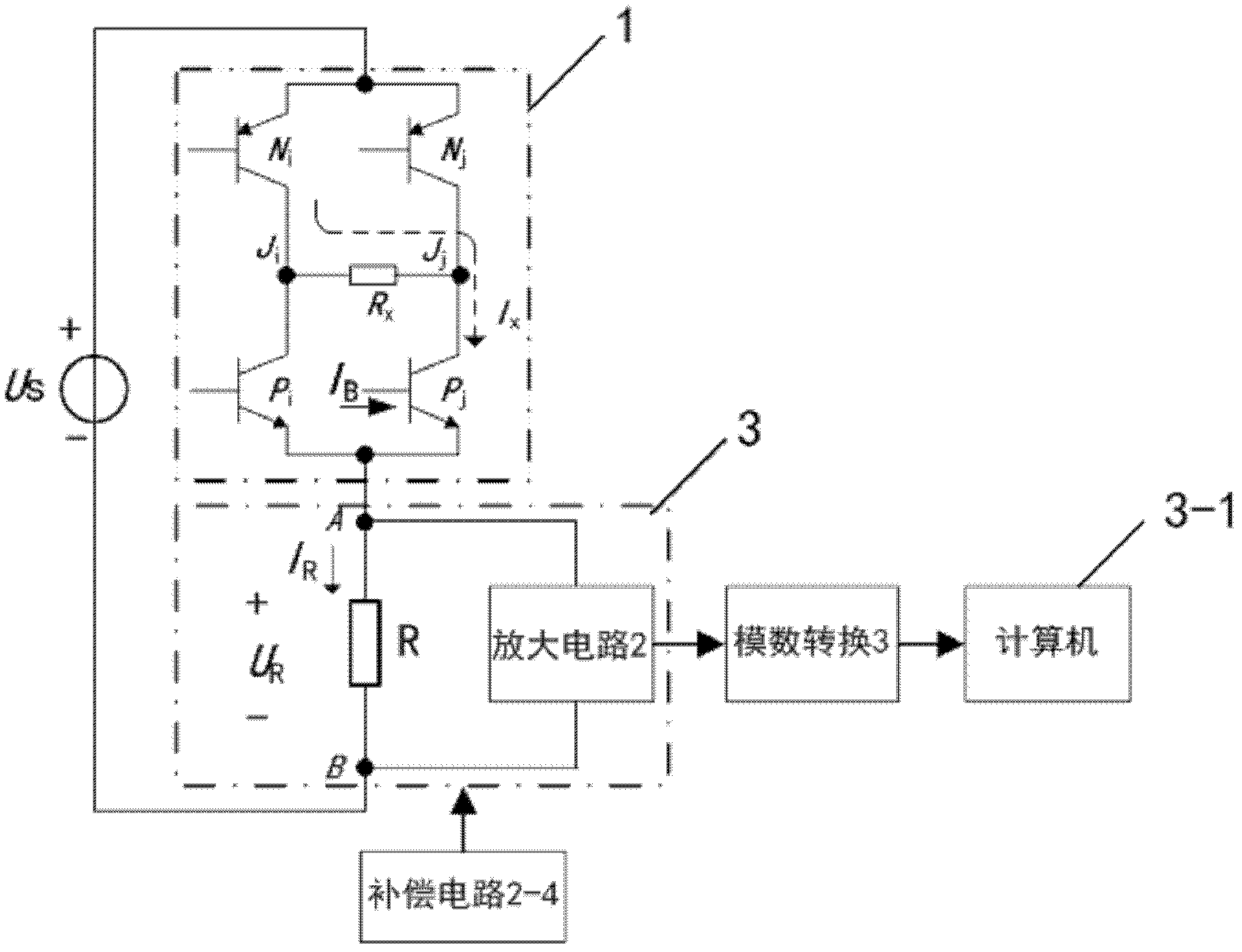
[0024] See figure 1 , a method for detecting circuit board circuit insulation, comprising using a circuit board insulation resistance testing circuit to detect circuit board insulation resistance, the detection steps comprising:
[0025] ① The measured insulation resistance R obtained from the triode array 1 X current I x and the base current I of the conduction transistors in the transistor array 1 B The sum flows into the sampling resistor R of the pre-circuit 3 to obtain the input voltage of the amplifying circuit 2 in the pre-circuit;
[0026] ② Set a compensation circuit 2-4 connected to the compensation terminal of the pre-circuit 3, the compensation circuit (2-4) generates a compensation voltage or current to eliminate the total output voltage Uo of the pre-circuit 3 error, which only refers to the base current I of the transistors in the conduction state in the transistor array 1 B The error generated by flowing into the sampling resistor R.
[0027] ③ Connect the...
Embodiment 2
[0029] See figure 1 , is suitable for implementing the scheme of the working method of the above-mentioned embodiment 1, the circuit board insulation resistance testing circuit, comprising: a triode array 1, a pre-circuit 3 composed of a sampling resistor R and an amplifying circuit 2, the pre-circuit 3 The compensation terminal is connected with a compensation circuit 2-4; and the compensation voltage or current generated by the compensation circuit 2-4 is suitable for eliminating the error of the total output voltage Uo of the pre-circuit 3, and this error only refers to the error caused by the The base current I of the triode in the conduction state in the triode array 1 B generated by flowing into the sampling resistor R.
Embodiment 3
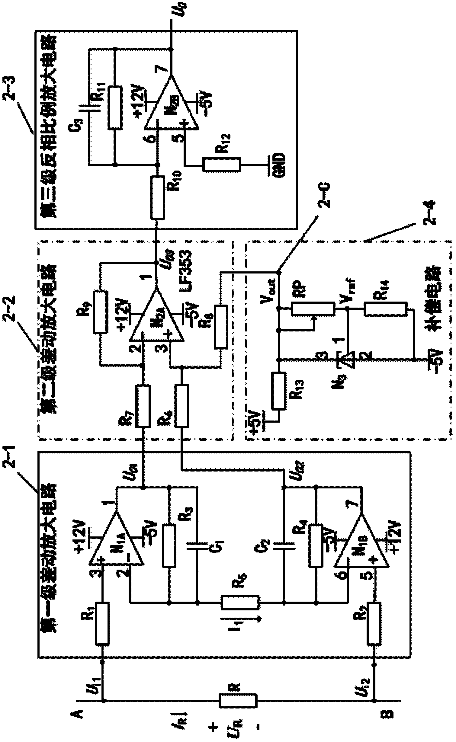
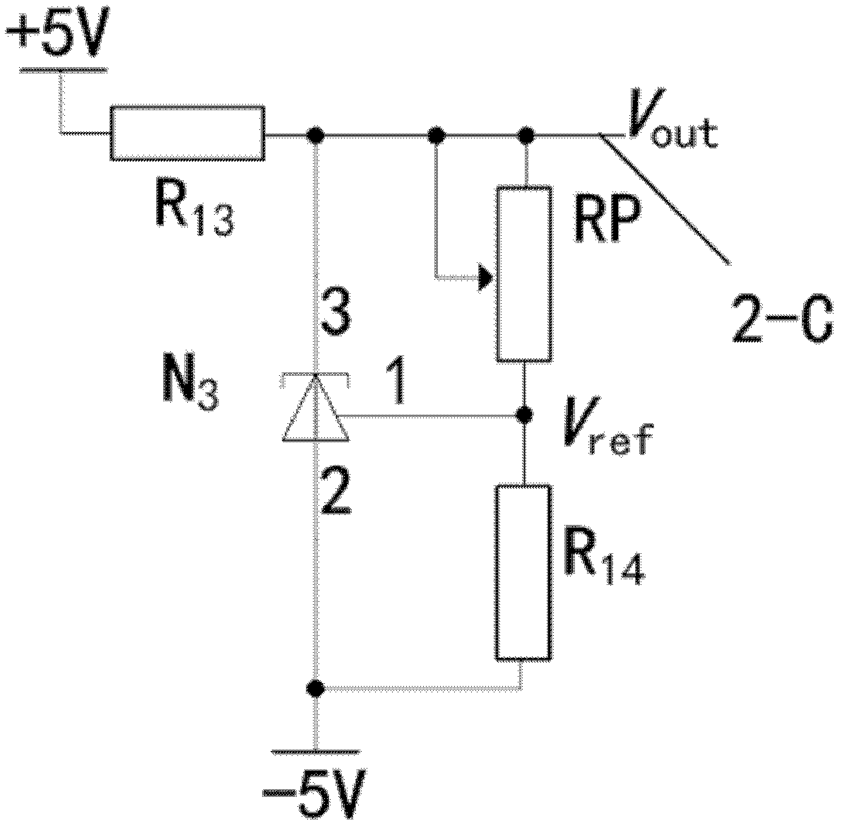
[0031] See figure 2 , 3 , as a solution to realize the above-mentioned embodiment 2, the amplifying circuit 2 is a multi-stage amplifying circuit, and the intermediate stage amplifying circuit is composed of an integrated operational amplifier, and the compensation terminal is the non-inverting terminal of the integrated operational amplifier, forming Non-inverting terminal voltage compensation.
PUM
 Abstract
Description
Claims
Application Information


