
thermal print head
A thermal print head and substrate technology, applied in printing and other directions, can solve problems such as increased damage to the protective layer
- Summary
- Abstract
- Description
- Claims
- Application Information
AI Technical Summary
Problems solved by technology
Method used
Image

Examples
Embodiment Construction
[0042] Preferred embodiments of the present invention will be described in detail below in conjunction with the accompanying drawings.
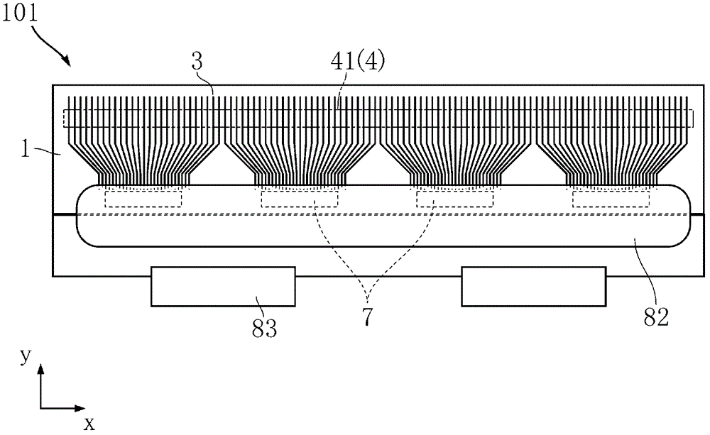
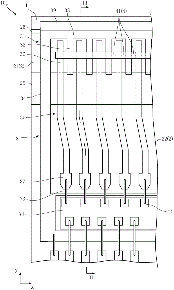
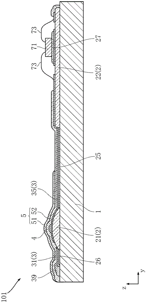
[0043] Figure 1 to Figure 5 is a thermal print head according to a first embodiment of the present invention. The thermal printhead 101 of this embodiment includes a substrate 1 , a glaze layer 2 , an electrode layer 3 , a resistor layer 4 , a protective layer 5 and a driver IC 71 . The thermal printhead 101 is a component mounted on a printer that prints on thermal paper for producing, for example, barcode sheets and receipts. In addition, for the convenience of understanding, figure 1 The protective layer 5 is omitted in .
[0044]The substrate 1 can be formed of ceramics such as Al2O3, and the thickness can be 0.6-1.0mm. Such as figure 1 As shown, the substrate 1 has a rectangular shape extending along the main scanning direction X. As shown in FIG. The substrate 1 may also have a structure of a wiring substrate in which a base la...
PUM
 Abstract
Description
Claims
Application Information