Production method of cavity PCB plate

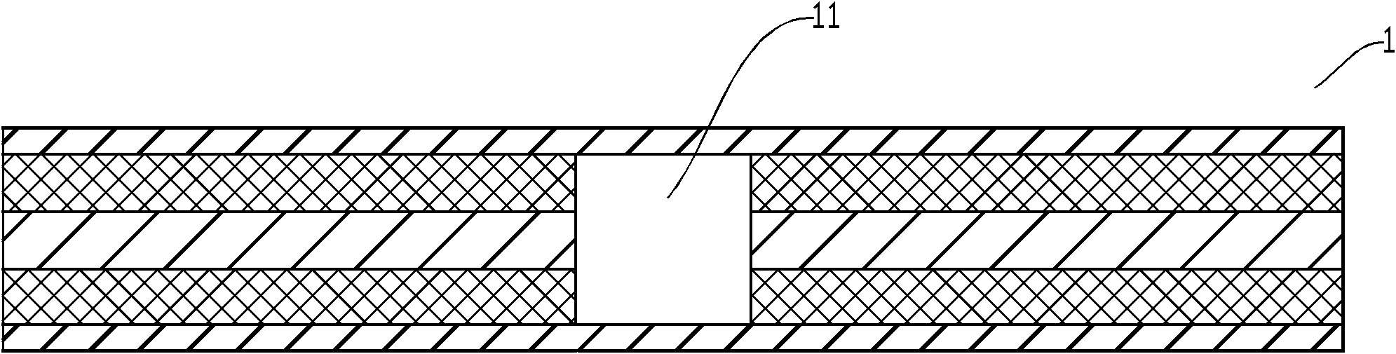
The technology of a PCB board and production method is applied in the field of cavity PCB board production, and can solve problems such as the size and shape of the cavity 11 not conforming, the difficulty of producing the cavity PCB board, and the flattening of the cavity, etc., and the method is convenient to implement, Less process, accurate size and depth effect

Inactive Publication Date: 2012-07-18
SHANGHAI MEADVILLE ELECTRONICS
View PDF2 Cites 13 Cited by
  • Summary
  • Abstract
  • Description
  • Claims
  • Application Information

AI Technical Summary

Problems solved by technology

like Figure 4 As shown, the balance of pressure and the soft properties of the press-fit pad will cause the first outer core plate 2 and the second outer core plate 6 at the cavity to sag into the cavity, resulting in the size and shape of the cavity 11 D

Method used


Image

  • Production method of cavity PCB plate
  • Production method of cavity PCB plate
  • Production method of cavity PCB plate

Examples


Embodiment 1

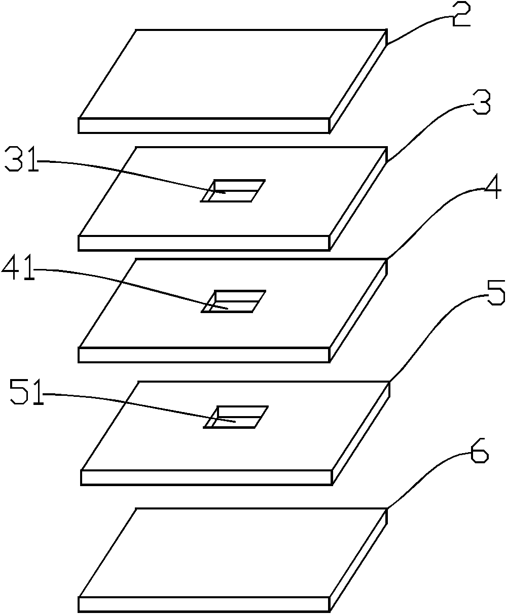
[0027] The production method of cavity PCB board comprises the following steps: as Figure 5 as shown,

[0028] a. The inner core board 4 is provided with a window 41 . A first prepreg 3 is pasted on the upper surface of the inner core board 4 , and a window 31 is opened in the first prepreg 3 . A second prepreg 5 is pasted on the lower surface of the inner core board 4 , and a window 51 is opened in the second prepreg 5 . Both the window 51 and the window 31 are aligned with the position of the window 41 .

[0029] b. Attaching the first outer layer core board 2 on the upper surface of the first prepreg 3 . For the convenience of description, marking lines 21 are marked on the upper surface of the first outer core board 2 , and the marking lines 21 do not need to be marked in actual production. The marking line 21 has the same size as the window 51 , the window 31 and the window 41 , and their positions are aligned. On the lower surface of the second prepreg 5, a second ...

Embodiment 2

[0039] On the basis of Embodiment 1, a piece of copper foil is provided between the first auxiliary board 91 and the first bonding pad 101 during lamination. A piece of copper foil is also disposed between the second auxiliary board 92 and the second bonding pad 102 . This can prevent the dust of the pressing pad from contaminating the board surface, and can also prevent the outer core board from being unevenly heated and affecting the performance of the circuit board.

Embodiment 3

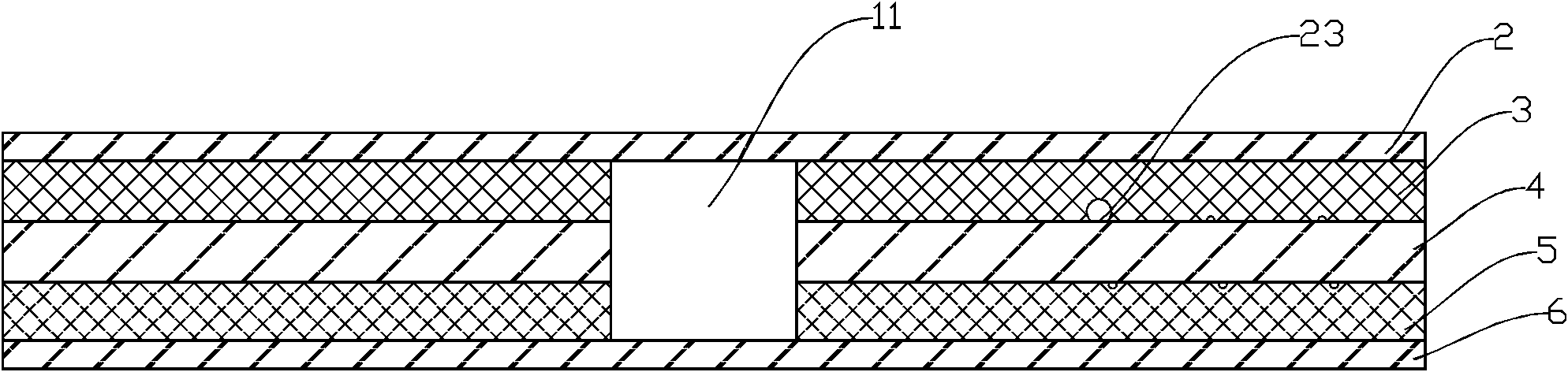
[0041] On the basis of Example 1, such as Figure 7 As shown, a first through hole 22 is drilled on the first outer core board 2 . The first through hole 22 communicates with the cavity 11 . A second through hole 62 is drilled on the second outer core board 6 , and the second through hole 62 communicates with the cavity 11 . Moreover, the first through hole 22 and the second through hole 62 can be arranged in a staggered manner.


PUM


Abstract

The invention discloses a production method of a cavity PCB plate. The method is characterized by comprising the following steps: a. respectively pasting a prepreg at each one of two surfaces of an internal layer core plate provided with a window, wherein both the two prepregs are respectively provided with a window which is aligned with the window of the internal layer core plate; b. pasting an external layer core plate at each surface of the two prepregs respectively; c. respectively arranging an accessory plate provided with a window at each surface of the two external layer core plates, wherein the window of each accessory plate is opposite to the window of the internal layer core plate; d. arranging a stitching pad at each surface of the two accessory plates respectively; e. carrying out lamination, and removing the stitching pads and the accessory plates to form the cavity PCB plate. According to the method, accurate positioning of a position of a cavity in the PCB plate can be realized, a dimension and a depth of the cavity in the plate are accurately ensured, and that a stereo structure of the cavity satisfies a requirement is ensured. The method has the advantages of being simple and effective and convenient enforcement, and is suitable for processing the PCB plate containing the cavity.

Description

technical field [0001] The invention relates to a production method of a cavity PCB board. Background technique [0002] like figure 1 As shown, it is a cavity PCB board 1 with a cavity 11 inside it. In the present invention, such a PCB board provided with a cavity is called a cavity PCB board for short. [0003] The production method of the cavity PCB board in the prior art is to attach a prepreg on the two surfaces of the inner core board respectively, and then attach an outer core board on the surface of the prepreg, and laminate at high temperature. Prepreg is mainly composed of thermoplastic resin, which is solid at room temperature and turns into semi-fluid liquid at high temperature. When returning to normal temperature after lamination, the prepreg will bond the multi-layer inner core board and the outer core board into one. When producing cavity PCB boards, such as figure 2 As shown, the cavity PCB 1 is made by laminating the first outer core board 2 , the fir...

Claims


Application Information

Patent Timeline
IPC IPC(8): H05K3/00
Inventor 屈刚赵国强陈晓峰黄伟曹立志
Owner SHANGHAI MEADVILLE ELECTRONICS
Why Eureka
Try Eureka