High-frequency vertical spring probe card structure

A vertical, probe card technology, applied in the field of probe structure, can solve the problems of imprecise production, high cost, inability to reach the probe, save time and cost, reduce signal interference, and quickly generate the process. Effect

Inactive Publication Date: 2012-07-25
PLEADER YAMAICHI
View PDF4 Cites 11 Cited by
  • Summary
  • Abstract
  • Description
  • Claims
  • Application Information

AI Technical Summary

Problems solved by technology

[0004] However, the above-mentioned existing probes still have many shortcomings. According to the manual assembly method of the prior art, the composition of each probe is time-consuming and labor-intensive, resulting in considerable cost. The contact end surface of the above-mentioned probes is a cylinder Three-dimensional shape, its production is not precise enough, assuming that the flatness is not good, it will affect the stability of the test; in addition, the shape limitation cannot meet the needs of thousands of manufactured and assembled probes today, and it is also impossible to realize the needle and probe. Needle spacing is reduced; what’s more, the above-mentioned probes are exposed too much and have no insulation, which is easy to generate extra capacitance and inductance, and is not suitable for high-frequency testing. Therefore, the present invention proposes a high-frequency vertical shrapnel probe. Needle card structure to improve the above problems

Method used


Image

  • High-frequency vertical spring probe card structure
  • High-frequency vertical spring probe card structure
  • High-frequency vertical spring probe card structure

Examples


Embodiment Construction

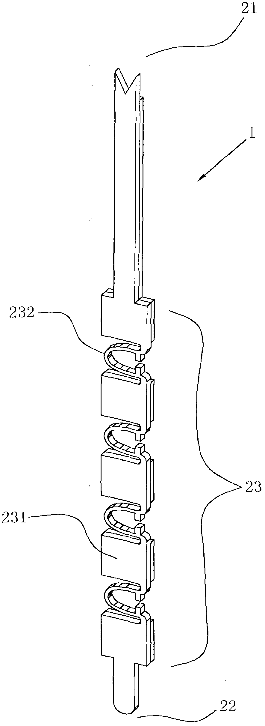
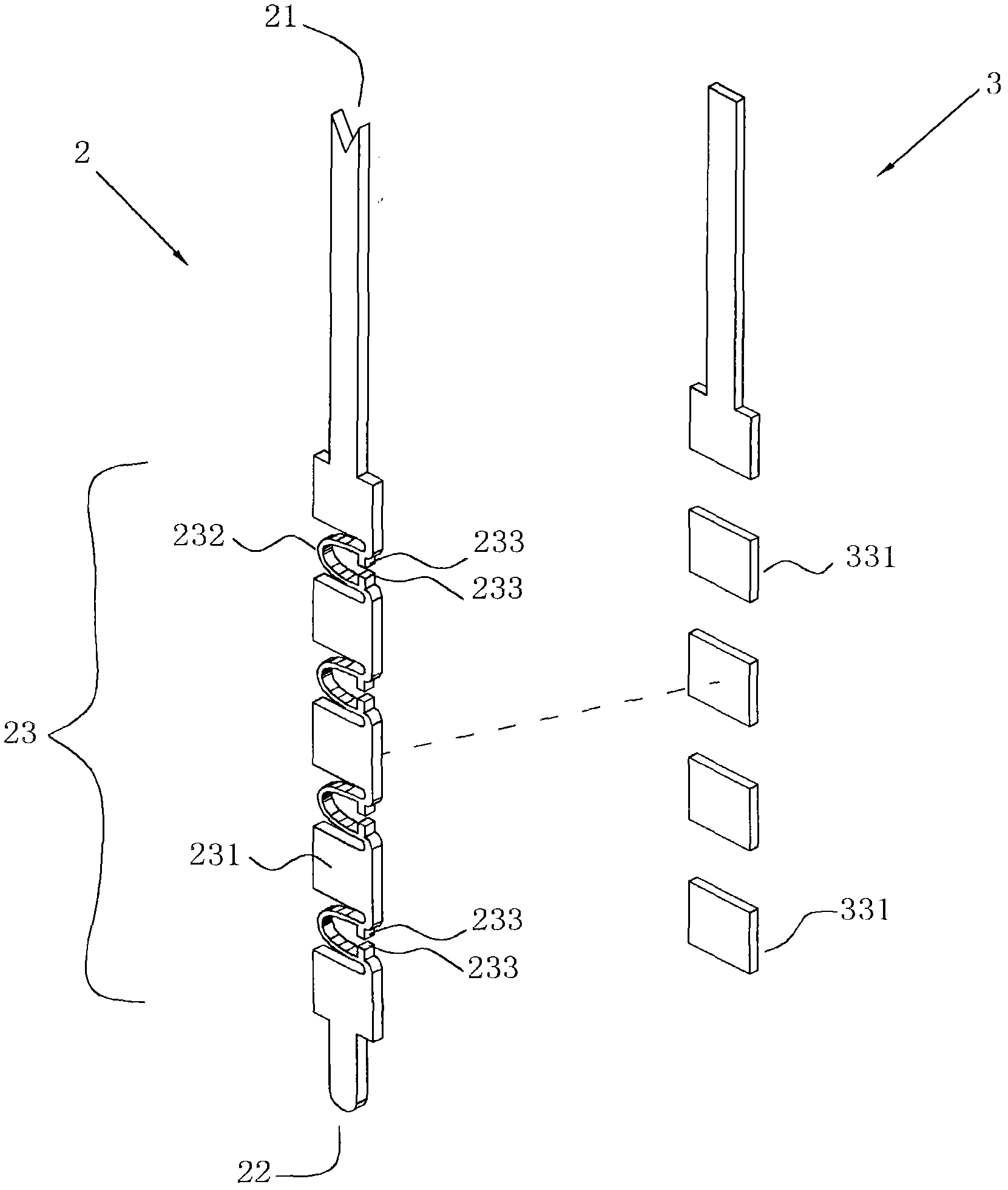
[0046] Please refer to figure 2 , figure 2 It is a combined schematic diagram of the structure of the first embodiment of the present invention. The probe 1 of the present invention has a first contact piece 21, a second contact piece 22 and a probe body 23, and the first contact piece 21 and the second contact piece 22 are used for electrical contact with an external member during pressure. Contact point; the probe body 23 has a plurality of plates 231 and a plurality of elastic bodies 232, which are interconnected and formed. The plurality of plates 231 are used to support the elasticity of the elastic body 232 when it is compressed in the vertical direction. variable. In addition, the flat design of the probes 1 is arranged in parallel, and the plane of the arrangement is the side of the probes (that is, the surface with a smaller surface area of ​​the probes). Through the neat parallel arrangement, the same area of ​​the component or circuit board to be tested can be t...


PUM


Abstract

The invention provides a high-frequency vertical spring probe card structure including a plurality of probes. Each of the probes includes at least one conducting layer and at least one insulating layer. The conducting layer includes a first contact end and a second contact end used for electrically contacting an external component while the probe is compressed and includes a probe body including at least one plate portion and at least one resilient portion connected to each other. The plate portion is used for supporting deformation of the resilient portion while the resilient portion is compressed vertically. The insulating layer includes at least one plate member tightly attached to the plate portion of the conducting layer correspondingly. The probe structure of the invention is simple and can be formed as multi-layer stack structure by electroplating through Lithographie GaVanoformung Abformung (LIGA) technology.

Description

technical field [0001] The invention relates to a probe structure, in particular to a high-frequency vertical shrapnel probe card structure, which is an innovative shape design of a micro-probe, which can be used in high-frequency and high-speed chip testing, and can be compressed longitudinally. When the elasticity is high, it still maintains a good contact state during the test. Background technique [0002] Before the chips in the semiconductor industry are packaged, they need to be supplemented with related testing instruments and software programs, and perform various functional tests on the bare crystal with probes, so as to screen out good and bad products, and good products are then processed. Packaging works. [0003] Due to the continuous evolution of integrated circuit manufacturing processes, the line width and spacing between circuits are shrinking day by day, and the requirements for probes used in testing have also changed from cantilever probes with curved t...

Claims


Application Information

Patent Timeline
Patent Type & Authority Applications(China)
IPC IPC(8): G01R1/06
CPCG01R1/06722G01R1/06744
Inventor 黄郑隆
Owner PLEADER YAMAICHI
Why Eureka
Try Eureka