Static discharging circuit

An electrostatic discharge circuit and voltage divider circuit technology, applied in circuit devices, emergency protection circuit devices for limiting overcurrent/overvoltage, emergency protection circuit devices, etc., can solve problems such as affecting the maximum electrostatic discharge capacity.

Inactive Publication Date: 2012-07-25
SHANGHAI AWINIC TECH CO LTD
View PDF4 Cites 6 Cited by
  • Summary
  • Abstract
  • Description
  • Claims
  • Application Information

AI Technical Summary

Problems solved by technology

[0012] The method of stacking MOS transistors in a common process can solve the withstand voltage problem of ESD devices, but since the ESD current passes through parasitic NPN transistors (such as image 3 shown in the parasitic NPN transistor Q2) to discharge, which seriously affects the ability of the maximum electrostatic discharge

Method used


Image

  • Static discharging circuit
  • Static discharging circuit
  • Static discharging circuit

Examples


Embodiment Construction

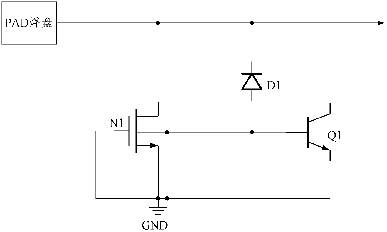
[0037] As mentioned in the background technology, in the prior art, the high-voltage resistance of devices formed by high-voltage technology or BCD technology is limited, and the ESD protection circuit using ordinary technology to stack MOS transistors solves the problem of high-voltage resistance, but it mainly uses parasitic NPN The triode releases the ESD current, which seriously affects its electrostatic discharge capability.

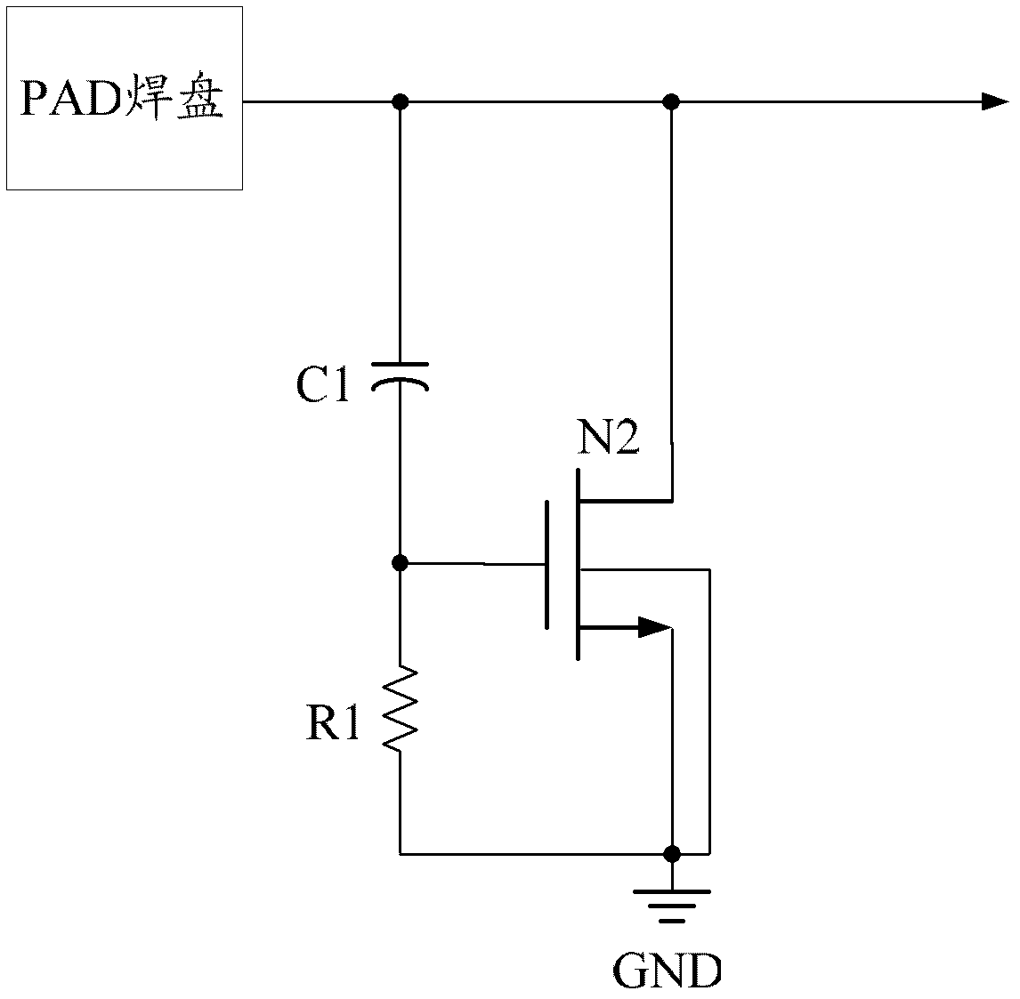
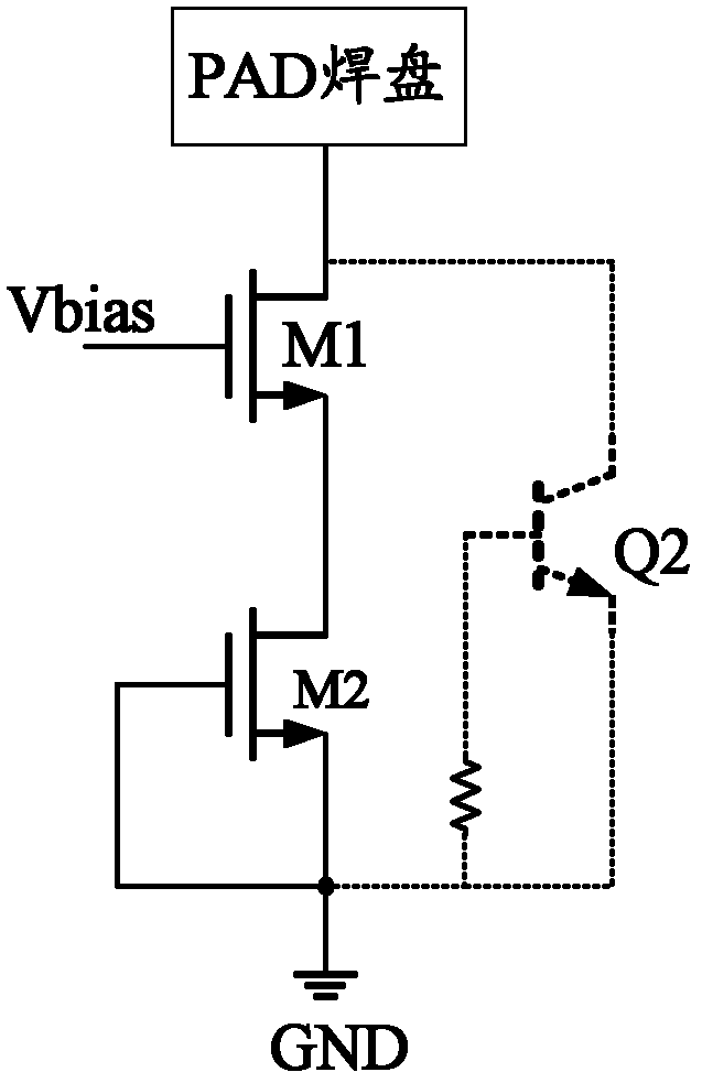
[0038]The electrostatic discharge circuit of the present invention includes a voltage divider circuit, a first NMOS transistor and a second NMOS transistor, and the voltage divider circuit is used to provide an appropriate bias voltage to the first NMOS transistor, so that the first NMOS transistor is in a conduction state; The second NMOS transistor is also quickly turned on during the ESD event, so that the first NMOS transistor and the second NMOS transistor form a path to quickly release the ESD current. In this circuit, the ESD current is relea...


PUM


Abstract

The invention relates to a static discharging circuit, which comprises a voltage division circuit, a first N-channel metal oxide semiconductor (NMOS) tube and a second NMOS tube, wherein a positive electrode input end of the voltage division circuit is connected with a high-voltage input end, a negative electrode input end of the voltage division circuit is coupled with the ground, and an output end is connected with a grid electrode of the first NMOS tube and is used for outputting bias voltage conducting the first NMOS tube; a drain electrode of the first NMOS tube is connected with the high-voltage input end, and a source electrode is connected with a drain electrode of the second NMOS tube; and a source electrode of the second NMOS tube is grounded, and a grid electrode of the second NMOS tube is coupled with the ground. The static discharging circuit has the advantages that the circuit voltage resistant value is improved, and meanwhile, the static discharging performance of the static discharging circuit is also improved.

Description

technical field [0001] The invention relates to the technical field of electronic circuits, in particular to an electrostatic discharge circuit. Background technique [0002] Electrostatic Discharge (ESD) is the main factor that causes most electronic components or electronic systems to be damaged by electrical overstress (Electrical Overstress, EOS), which can cause permanent damage to semiconductor devices, resulting in integrated circuit function failure. At present, integrated circuits are mainly based on complementary metal oxide semiconductor (CMOS). In order to prevent integrated circuits from being damaged by ESD, ESD circuits are usually designed in the circuit. [0003] figure 1 A schematic diagram of an ESD protection circuit with a GGNMOS structure in the prior art is shown. refer to figure 1 , the ESD protection circuit of the GGNMOS (Gate Grounded NMOS, gate grounded NMOS) structure includes an NMOS transistor N1. The source, gate and substrate of the NMOS...

Claims


Application Information

Patent Timeline
Patent Type & Authority Applications(China)
IPC IPC(8): H02H9/04
Inventor 孔庆河丁俊张振浩
Owner SHANGHAI AWINIC TECH CO LTD
Why Eureka
Try Eureka