Semiconductor wafer liquid-spraying etching system and method

A semiconductor and wafer technology, applied in the field of semiconductor wafer spray etching system, can solve the problems of poor etching uniformity, inability to adjust, affecting the quality of chip processing, etc. The effect of etching efficiency and product quality

Inactive Publication Date: 2012-08-01
NANTONG FUJITSU MICROELECTRONICS
View PDF5 Cites 9 Cited by
  • Summary
  • Abstract
  • Description
  • Claims
  • Application Information

AI Technical Summary

Problems solved by technology

[0003] This approach poses a problem of poor etch uniformity, for example, in figure 1 Among them, the surface of the wafer 11 is usually not completely smooth, but has certain unevenness. When the etchant is sprayed onto the surface of the wafer 11, the dosage of the concave and the convex is different, resulting in uneven etching, and the etching is close to the spraying. The position of the point is etched severely
another example figure 2 As shown, when t

Method used


Image

  • Semiconductor wafer liquid-spraying etching system and method
  • Semiconductor wafer liquid-spraying etching system and method
  • Semiconductor wafer liquid-spraying etching system and method

Examples


Embodiment approach

[0028] refer to Figure 7 , the present invention also provides a semiconductor wafer liquid spray etching method based on the above-mentioned semiconductor wafer liquid spray etching system, one embodiment of which includes the following steps:

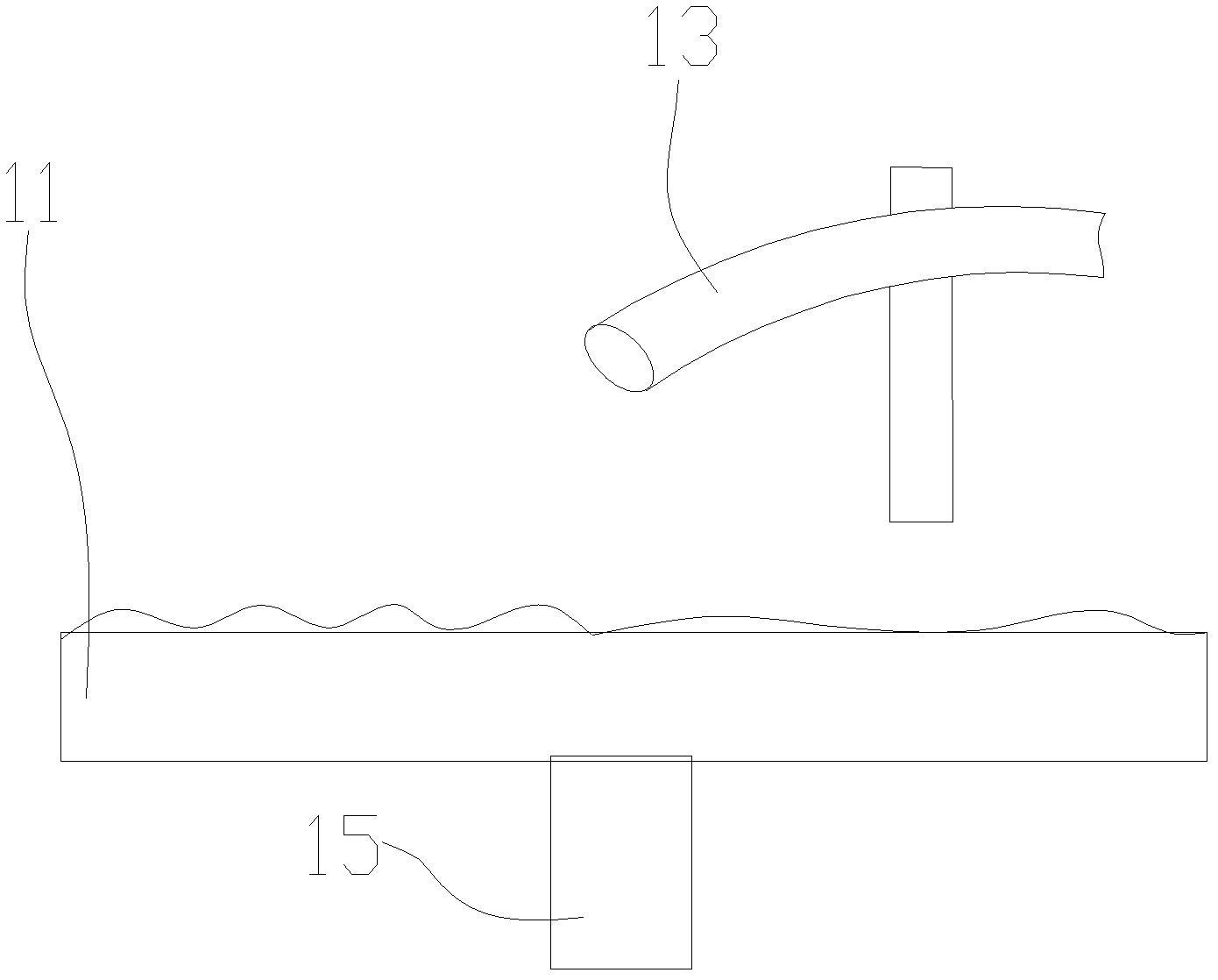
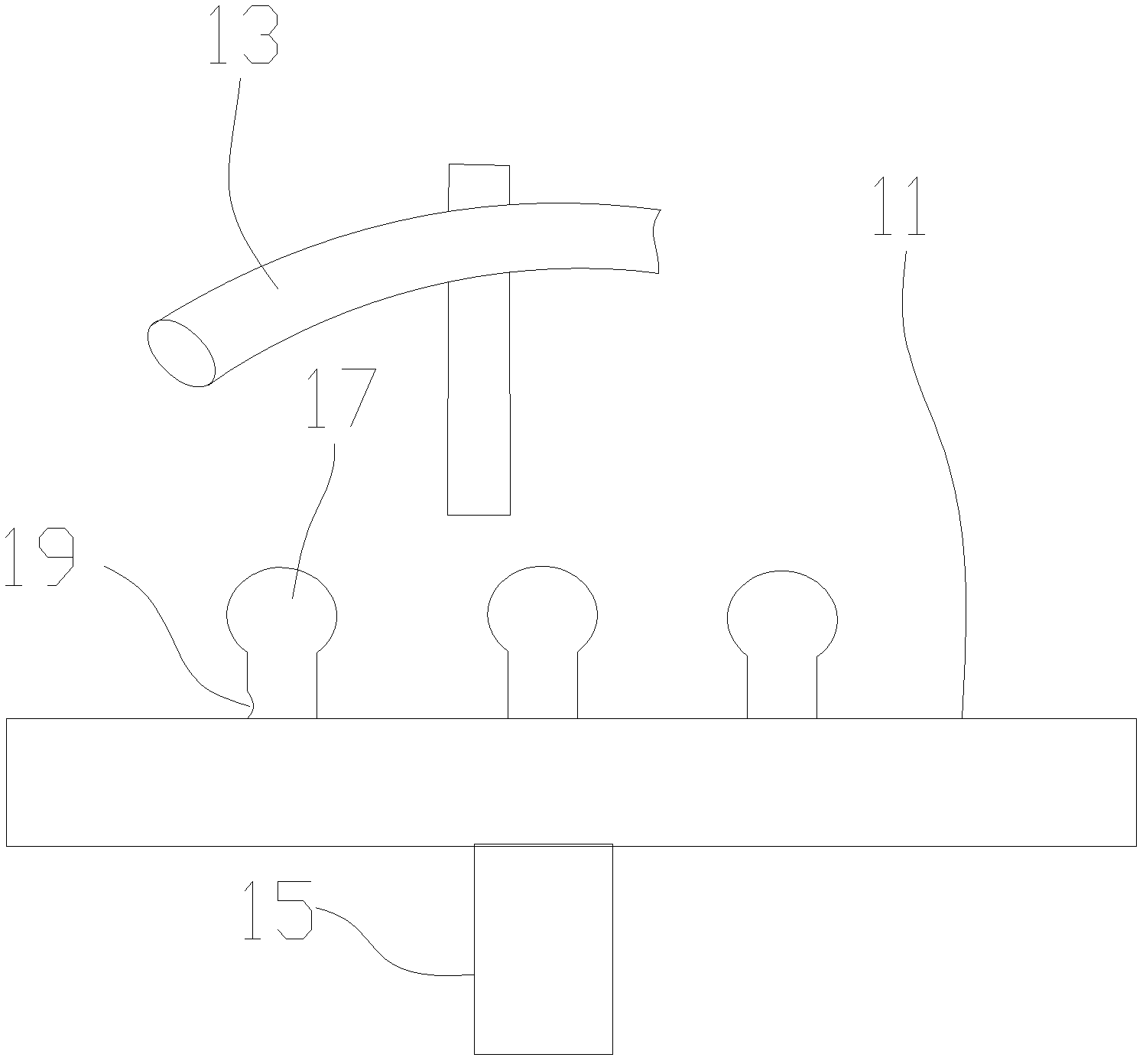
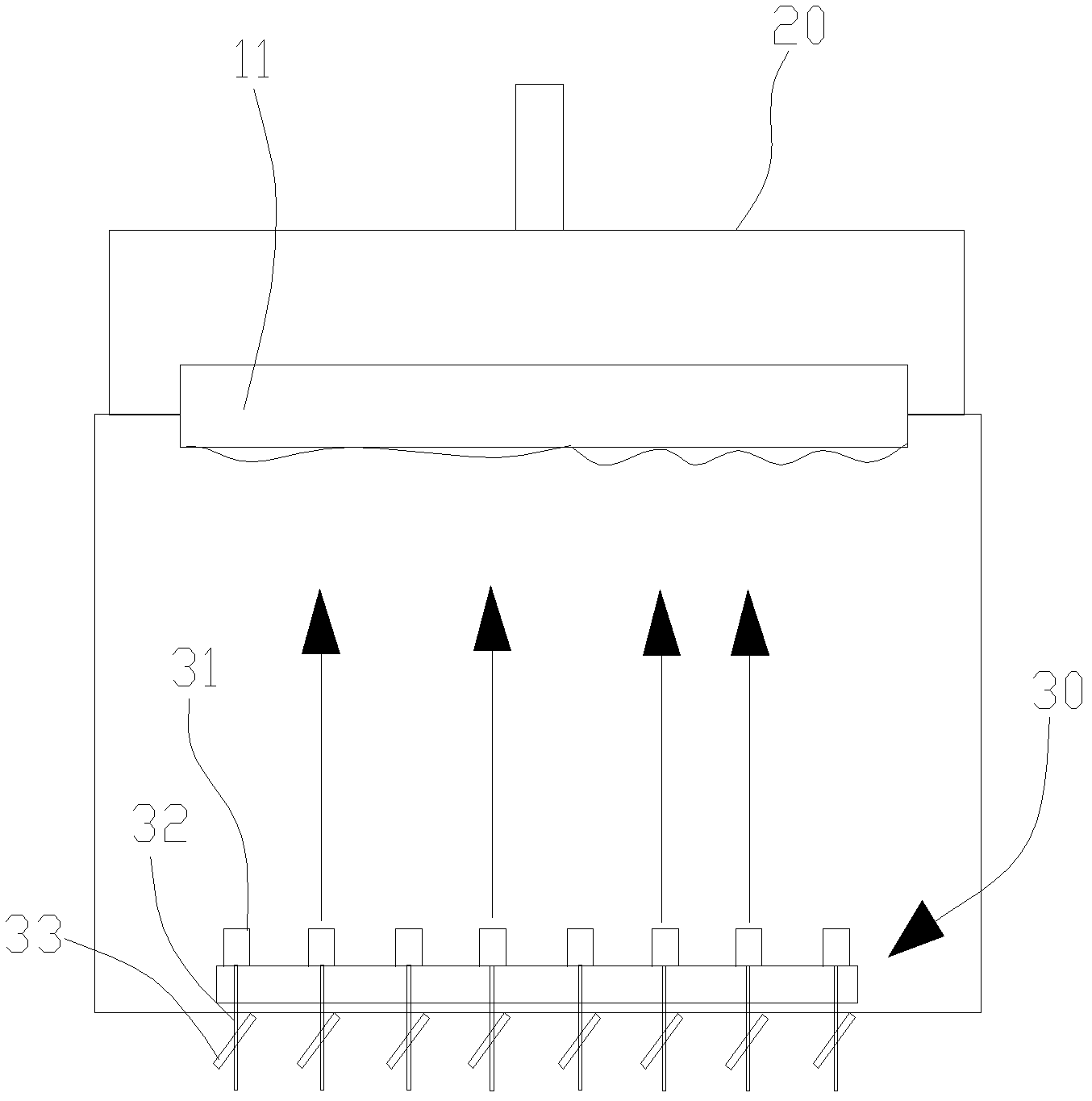
[0029] Step S1 : Fix the semiconductor wafer 11 with its surface to be etched facing down on the stage device 20 , and control the rotation of the semiconductor wafer 11 through the stage device 20 .

[0030] Step S2: adjust the flow rate of each nozzle 31 on the spraying device 30 through each control member of the spraying device 30, and spray the etching solution upwards to the corresponding position of the surface to be etched of the semiconductor wafer 11 through the above-mentioned multiple nozzles 31.

[0031] Optionally, in step S2, in the semiconductor wafer liquid jet etching method, the flow rate of the nozzles is controlled by operating the solenoid valves 33 provided on the delivery pipes 32 of the nozzles 31 .

[0032]...


PUM


Abstract

The invention relates to a liquid-spraying etching system and method of a semiconductor wafer. The semiconductor wafer liquid-spraying etching system comprises a carrying-platform device and a spraying device, wherein the carrying-platform device is used for fixing the semiconductor wafer when the surface to be etched of the semiconductor wafer faces downwards, and controlling rotation of the semiconductor wafer; the spraying device is placed below the carrying-platform device and comprises a plurality of spraying nozzles and a plurality of controlling pieces; all the spraying nozzles are used for spraying etching liquid on the corresponding positions of the surface to be etched on the semiconductor wafer upwards; the plurality of controlling pieces correspond to the plurality of spraying nozzles; and each controlling piece is used for controlling the spraying flow rate of the etching liquid of the spraying nozzle corresponding to the control piece. The liquid-spraying etching system and method have good etching uniformity and can improve the quality of products.

Description

technical field [0001] The invention relates to a semiconductor wafer etching system and method, in particular to a semiconductor wafer liquid jet etching system and method. Background technique [0002] In the chip manufacturing process, an etching process is required to remove a certain material, such as photoresist, from the surface of the wafer. One method of the etching process is to use an etching solution on the surface of the wafer to remove the material on the surface of the wafer. . refer to figure 1 and figure 2 The traditional way of this method is to fix the wafer 11 on the processing table 15, the nozzle 13 above the wafer 11 sprays the etching liquid downward, and the centrifugal force generated by the rotating wafer 11 diffuses the etching liquid outward. [0003] This approach poses a problem of poor etch uniformity, for example, in figure 1 Among them, the surface of the wafer 11 is usually not completely smooth, but has certain unevenness. When the et...

Claims


Application Information

Patent Timeline
IPC IPC(8): H01L21/306B05B13/02B05B1/30
Inventor 丁万春
Owner NANTONG FUJITSU MICROELECTRONICS
Why Eureka
Try Eureka