Memory device and manufacturing method therefor

A technology of a storage device and a manufacturing method, which is applied in information storage, static memory, digital memory information, etc., can solve the problems of uneven film thickness, abnormal shape, and uneven electrical characteristics of resistance change elements such as initial resistance value, etc., and achieve reduction Effect of less unevenness and initial resistance value unevenness

Active Publication Date: 2014-12-10
PANASONIC SEMICON SOLUTIONS CO LTD
View PDF5 Cites 0 Cited by
  • Summary
  • Abstract
  • Description
  • Claims
  • Application Information

AI Technical Summary

Problems solved by technology

[0029] Considering how this dependence is reflected in the characteristics of the actual variable resistance element, in the variable resistance element in which the conductive via hole is formed, it is unavoidable that the film thickness of the upper electrode is not uniform when the contact hole is formed (due to exposure to the contact hole). The film thickness of the upper electrode in the region within is thinner than other regions) occurs
Therefore, the occurrence of non-uniformity in the initial resistance value of the resistance variable element cannot be avoided, which is not preferable.
[0030] As mentioned above, due to the abnormal shape of the joint portion of the upper electrode and the conductive via hole, and the unevenness of the film thickness of the upper electrode due to the overetching at the time of forming the contact hole for forming the conductive via hole, the initial resistance value, etc. There is also non-uniformity in the electrical characteristics of the variable resistance element

Method used


Image

  • Memory device and manufacturing method therefor
  • Memory device and manufacturing method therefor
  • Memory device and manufacturing method therefor

Examples


Embodiment approach 1

[0071] [Storage Device Configuration]

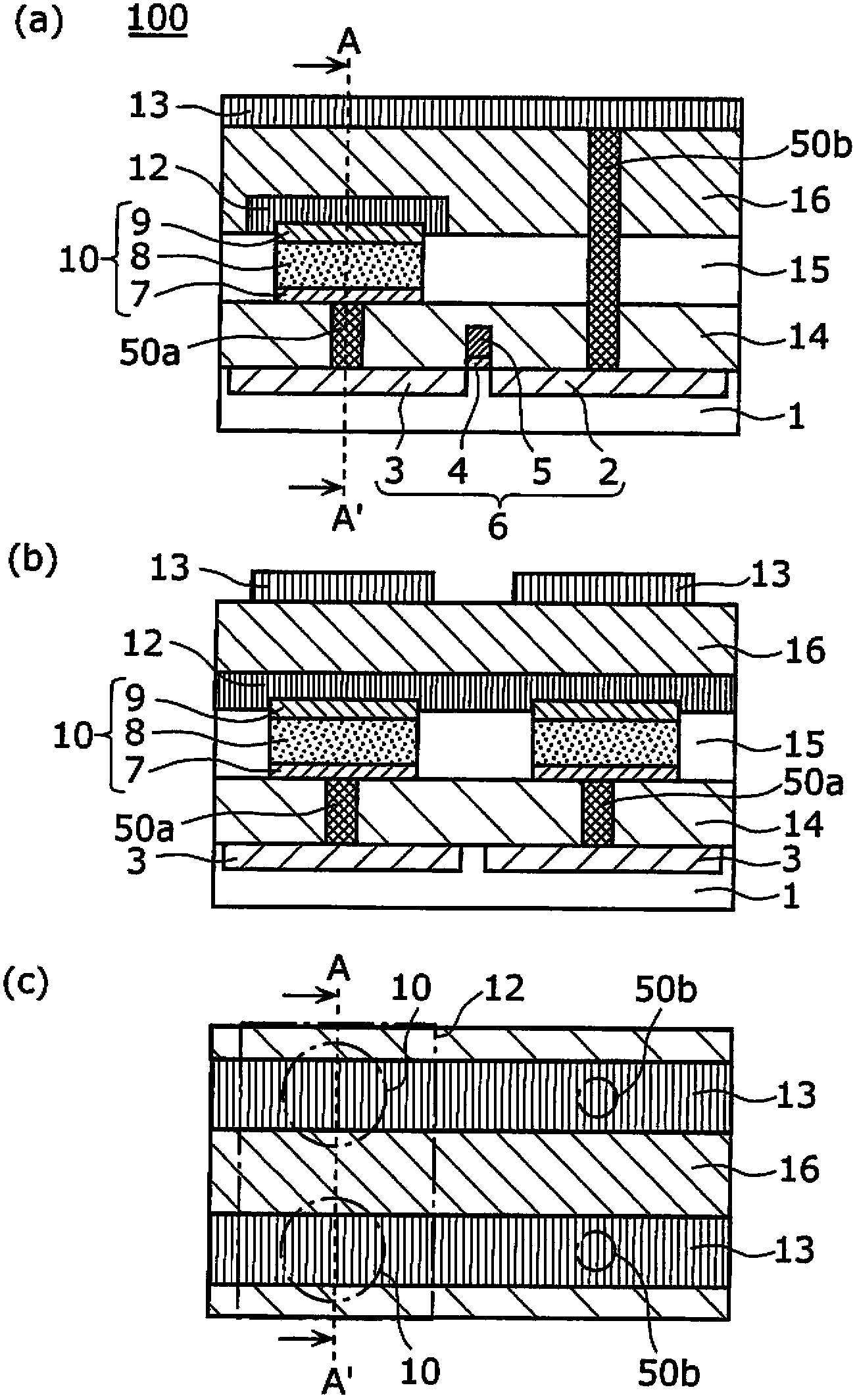
[0072] figure 1 is a schematic diagram of the storage device according to Embodiment 1, figure 1 (a) is a schematic cross-sectional view showing the configuration of the storage device 100 , figure 1 (b) is viewed from the direction of the arrow figure 1 (a) A schematic sectional view of the section along line A-A', figure 1 (c) is a schematic plan view of the same figure (a) viewed from the surface. In addition, in figure 1 In (c), some constituent elements of the memory device that are not visible on the surface are indicated by dashed-dotted lines and given reference numerals.

[0073] The memory device 100 includes a plurality of 1T1R memory cells. In detail, the memory cell is formed by connecting the selection transistor 6 and the variable resistance element 10 in series through the conductive via 50a. The selection transistor 6 is composed of the source region 2, the drain region 3, and the gate electrode 5. The source...

Embodiment approach 2

[0127] [Storage Device Configuration]

[0128] The memory device 200 of the second embodiment differs from the memory device 100 of the first embodiment in that when the lead wire 12 is formed, the metal wire 17 connected to other than the upper electrode 9 is formed simultaneously with the formation of the lead wire 12 . The other configurations are the same as those of the storage device 100 according to Embodiment 1, and therefore description thereof will be omitted.

[0129] Image 6 is a schematic diagram of the storage device 200 according to Embodiment 2, Image 6 (a) is a schematic cross-sectional view showing the configuration of the storage device 200 , Image 6 (b) Viewed from the direction of the arrow Image 6 (a) A schematic sectional view of the section along line BB', Image 6 (c) is a schematic plan view of the same figure (a) viewed from the surface. In addition, in Image 6 In (c), some constituent elements of the memory device that are not visible on ...

Embodiment approach 3

[0148] [Storage Device Configuration]

[0149] The memory device 300 of the third embodiment differs from the memory device 100 of the first embodiment in that the lead wiring 12 is in contact with the variable resistance layer 8 in addition to the upper electrode 9 of the variable resistance element 10 , and the other configurations are the same as those of the first embodiment. The storage device 100 is the same, so the description is omitted.

[0150] Figure 8 is a schematic diagram of the storage device 300 according to Embodiment 3, Figure 8 (a) is a schematic cross-sectional view showing the configuration of the storage device 300 . also, Figure 8 (b) is viewed from the direction of the arrow Figure 7 (a) Schematic sectional view of the section along line C-C'. exist Figure 8 (a), for Figure 1 ~ Figure 3 The same constituent elements are assigned the same reference numerals, and description thereof will be omitted.

[0151] The memory device 300 includes a ...


PUM


Abstract

Disclosed is a memory device provided with a plurality of memory cells and a lead-out line (12) shared among the memory cells. Each memory cell is provided with a transistor (6) formed above a substrate (1) and a variable resistance element (10) having a lower electrode (7), an upper electrode (9) that comprises a noble metal, and a variable resistance layer (8) disposed between the lower electrode (7) and the upper electrode (9). The resistance value of the variable resistance layer (8) changes reversibly in response to electric pulses that go through the transistor (6) and are applied between the lower electrode (7) and the upper electrode (9). The lead-out line (12) is in direct contact with the upper electrodes (9) of the memory cells.

Description

technical field [0001] The present invention relates to a memory device having a memory cell composed of a so-called variable resistance element whose resistance value changes reversibly based on an electric signal and a transistor, and a method for manufacturing the same. Background technique [0002] In recent years, research and development have been conducted on memory devices having memory cells configured using so-called variable resistance elements. Here, the variable resistance element refers to an element that has a property of changing its resistance value reversibly by an electric signal and that can store information corresponding to the resistance value in a non-volatile manner. [0003] As a memory device using such a variable resistance element, there is known a memory device having a structure in which a series-connected A MOS transistor and a variable resistance element are called 1T1R (1 transistor 1 resistor) type memory cells (for example, refer to Paten...

Claims


Application Information

Patent Timeline
Patent Type & Authority Patents(China)
IPC IPC(8): H01L27/105H01L27/10H01L45/00H01L49/00
CPCH01L45/08H01L45/1675G11C2213/79H01L27/2436H01L27/2463G11C13/0007H01L45/146H01L27/101H01L45/04H01L45/1233H10B63/30H10B63/80H10N70/24H10N70/20H10N70/826H10N70/8833H10N70/063
Inventor 有田浩二三河巧
Owner PANASONIC SEMICON SOLUTIONS CO LTD
Why Eureka
Try Eureka