Array substrate, manufacture method thereof, display panel and display device

A technology for array substrates and display panels, applied in semiconductor/solid-state device manufacturing, instruments, semiconductor devices, etc., can solve problems such as increased cost, weakened electromagnetic wave intensity, and reduced spatial magnetic flux rate of change.

Active Publication Date: 2015-05-06
BOE TECH GRP CO LTD +1
View PDF5 Cites 0 Cited by
  • Summary
  • Abstract
  • Description
  • Claims
  • Application Information

AI Technical Summary

Problems solved by technology

[0007] 1) Adjust and reduce the amplitude of the high / low level (that is, the driving voltage value) loaded on the outer leads of the plurality of grid lines respectively. Since the change of the amplitude affects the intensity of the space electromagnetic wave, when the When the amplitude decreases, the intensity of the space electromagnetic wave also weakens, that is, the rate of change of the space magnetic flux decreases, which in turn affects the electric field of the edge pixel unit close to the outer lead of the grid line in the effective display area of ​​the display panel, so that the The width of the white line becomes narrower or lighter, but this solution does not make said white line disappear
[0008] 2) Increasing the spacing between the outer leads of the plurality of gate lines, so that the intensity of electromagnetic waves in a unit space is weakened, thereby affecting the pixel units at the edge of the outer leads of the plurality of gate lines in the effective display area of ​​the display panel. electric field, making the width of the white line narrow or even disappear, but this solution will greatly increase the size of the peripheral area of ​​the display panel, thus greatly reducing the utilization rate of the peripheral area of ​​the display panel and increasing the cost
[0009] 3) Adjust the timing of the backlight (B / L, back light) and the display panel and increase the delay of the backlight, that is, when the display panel is powered on and initialized, the backlight is not lit, and the backlight is turned on when the display panel works normally , this solution can prevent customers from seeing the white line from the perspective of visual observation, but it does not fundamentally solve the problem of the white line
[0010] It can be seen that none of the above solutions fundamentally solves the problem of the white line

Method used


Image

  • Array substrate, manufacture method thereof, display panel and display device
  • Array substrate, manufacture method thereof, display panel and display device
  • Array substrate, manufacture method thereof, display panel and display device

Examples


Embodiment 1

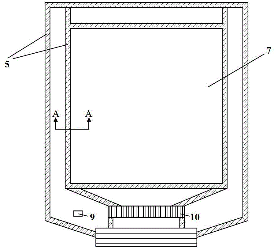
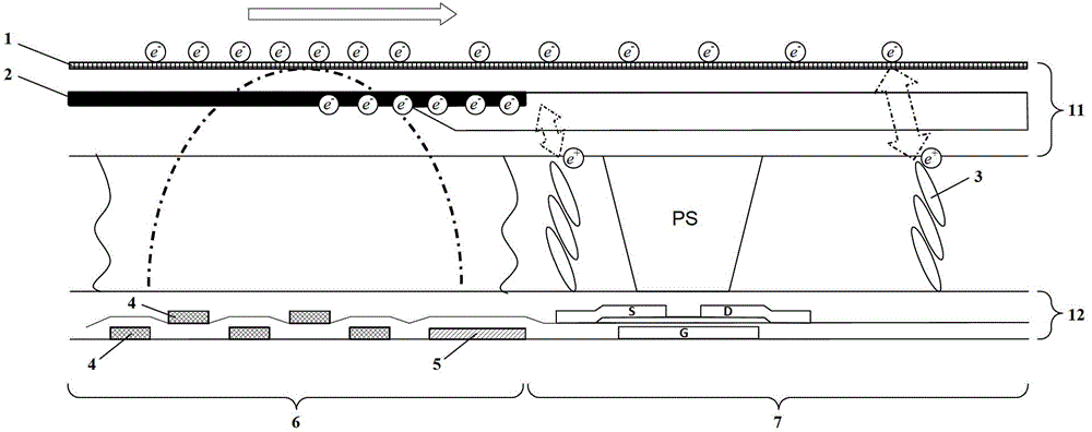
[0040] In this embodiment, the array substrate includes a plurality of gate lines, a plurality of data lines, a common electrode and a shielding layer. Wherein, each gate line and data line includes an outer lead, which are respectively called the outer lead of the gate line and the outer lead of the data line, and the number of the outer lead of the gate line is the same as that of the gate line, and the outer lead of the data line is the same as the number of the data line. The same number; the common electrode includes a plurality of outer leads, called the outer leads of the common electrode.

[0041] The shielding layer is arranged above the outer leads of the plurality of grid lines and connected to the grounding point, and is used for shielding space electromagnetic wave radiation excited by voltage changes in the outer leads of the plurality of grid lines. Preferably, the shielding layer covers the outer leads of the plurality of gate lines, and the shielding layer and...

Embodiment 2

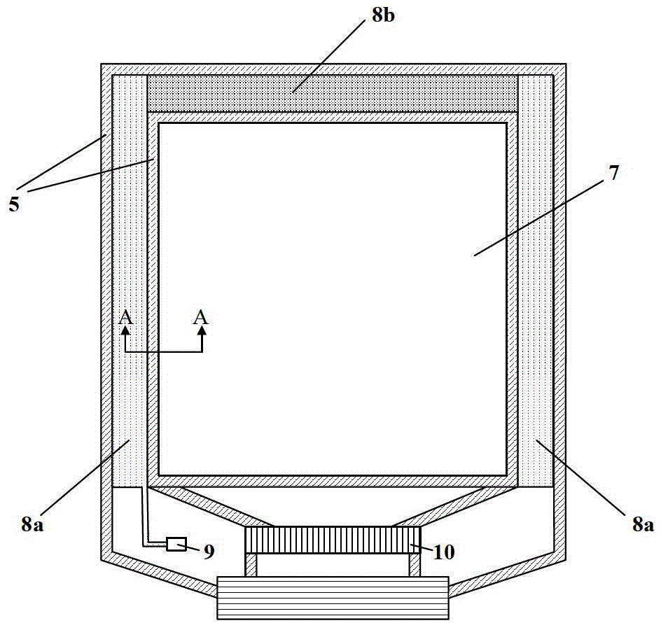
[0056] The difference between this embodiment and Embodiment 1 is that in this embodiment, the array substrate does not include the connection layer 8b, and the shielding layer 8a is respectively arranged on the left and right sides of the effective display area 7 above the outer leads 4 of the plurality of gate lines. Connect to two ground points respectively.

[0057] Other structures, methods, and functions in this embodiment are the same as those in Embodiment 1, and will not be repeated here.

Embodiment 3

[0059] Such as Figure 5 As shown, the difference between this embodiment and Embodiment 1 is that in this embodiment, the connection layer 8b is disposed above the outer leads of multiple data lines. Specifically, the connection layer 8b is disposed above the outer leads of the multiple data lines located at the bottom of the effective display area 7, that is, the shielding layer 8a and the connection layer 8b form a U-shaped structure.

[0060] Preferably, the connection layer 8b covers the outer leads of the plurality of data lines, and the connection layer 8b and the outer leads of the plurality of data lines are not electrically connected to each other. Further preferably, the insulating layer in the array substrate is also disposed between the connection layer 8b and the outer leads of the multiple data lines, so that the connection layer 8b and the outer leads of the multiple data lines are not electrically connected to each other.

[0061]In this embodiment, the width...


PUM


Abstract

Provided is an array substrate (12). The array substrate (12) comprises: a plurality of gate lines, each gate line comprising an outer lead (4); and a shielding layer (8a), the shielding layer (8a) being arranged above the outer leads (4) of the plurality of gate lines and connected to a ground point and used for shielding from the spatial electromagnetic wave radiation excited by the change of voltage in the outer leads (4) of the plurality of gate lines. The array substrate (12) can avoid the phenomenon that white lines appear on the left and right sides of a valid display region (7) on a display panel due to the excited spatial electromagnetic wave radiation upon the start-up initialization of a display device.

Description

technical field [0001] The invention belongs to the technical field of display manufacturing, and in particular relates to an array substrate, a method for manufacturing the array substrate, a display panel including the array substrate, and a display device including the display panel. Background technique [0002] With the development of display manufacturing technology, liquid crystal display technology has developed rapidly, and has gradually replaced traditional picture tube displays and become the mainstream of future flat panel displays. In the field of liquid crystal display technology, TFT-LCD (Thin Film Transistor Liquid Crystal Display) is widely used in televisions, computers, Mobile phones and other fields. [0003] Among them, the ADSDS (ADvanced Super Dimension Switch, referred to as ADS) type TFT-LCD has high resolution, high transmittance, low power consumption, wide viewing angle, high aperture ratio, low color difference, and no crowding. Advantages such...

Claims


Application Information

Patent Timeline
Patent Type & Authority Patents(China)
IPC IPC(8): G02F1/1362G02F1/1368G02F1/1343H01L23/552H01L21/77
CPCG02F1/136204G02F1/133388G02F1/136218
Inventor 李卿硕
Owner BOE TECH GRP CO LTD
Why Eureka
Try Eureka