Display panel, manufacturing method thereof, and display device

A technology for display panels and array substrates, applied in nonlinear optics, instruments, optics, etc., can solve problems such as poor image quality, prone to light leakage, and reduce the aperture ratio of unit pixels, so as to reduce the width, increase the cost, and improve the aperture rate effect

Active Publication Date: 2015-09-23
BOE TECH GRP CO LTD +1
View PDF5 Cites 0 Cited by
  • Summary
  • Abstract
  • Description
  • Claims
  • Application Information

AI Technical Summary

Problems solved by technology

Since the data line charges the pixel electrodes of each scanning line in turn, its own voltage will constantly change, resulting in the voltage difference of the electric field between the pixel electrode and the data line and the voltage difference of the electric field between the common electrode and the data line. change, and the RMS (Root Mean Square) value of the voltage difference between the electric field between the pixel electrode and the data line and the electric field between the common electrode and the data line is in the middle state rather than the extreme value, resulting in each data line The liquid crystal molecules above and on both sides of each data line cannot be effectively deflected. For a normally white mode display panel, since the RMS value cannot be at a maximum value, the liquid crystal molecules above and on both sides of each data line cannot be deflected. to an upright state (relative to the substrate); for normally black mode display panels, since the RMS value cannot be at a minimum value, the liquid crystal molecules above and on both sides of each data line cannot be deflected to a horizontal state ( Relative to the substrate), therefore, whether it is a normally white mode display panel or a normally black mode display panel for dark state inspection, light leakage is very easy to occur when viewed from the side or pressed, resulting in poor image quality
[0007] In order to overcome the above defects, in the prior art, the method of increasing the width of the black matrix in the color filter substrate is generally used to avoid or reduce light leakage, but this method will inevitably reduce the aperture ratio of the unit pixel

Method used


Image

  • Display panel, manufacturing method thereof, and display device
  • Display panel, manufacturing method thereof, and display device
  • Display panel, manufacturing method thereof, and display device

Examples


Embodiment 1

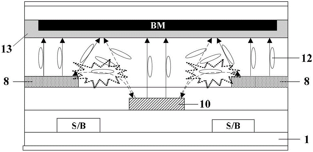
[0055] In this embodiment, the display panel adopts a normally white display panel, that is, when no voltage is applied to the display panel (there is no electric field or a weak electric field is formed between the pixel electrode and the common electrode), the effective display of the display panel corresponding to the liquid crystal molecules area (the display panel can usually be divided into two parts, that is, the effective display area and the peripheral area) transmit light; when a voltage is applied (a strong electric field is formed between the pixel electrode and the common electrode), the effective display area of ​​the display panel corresponding to the liquid crystal molecules does not Translucent.

[0056] In this embodiment, the display panel includes an array substrate and a color filter substrate; the array substrate includes a plurality of gate lines, a plurality of data lines, and a plurality of common electrode lines, and the plurality of gate lines and the...

Embodiment 2

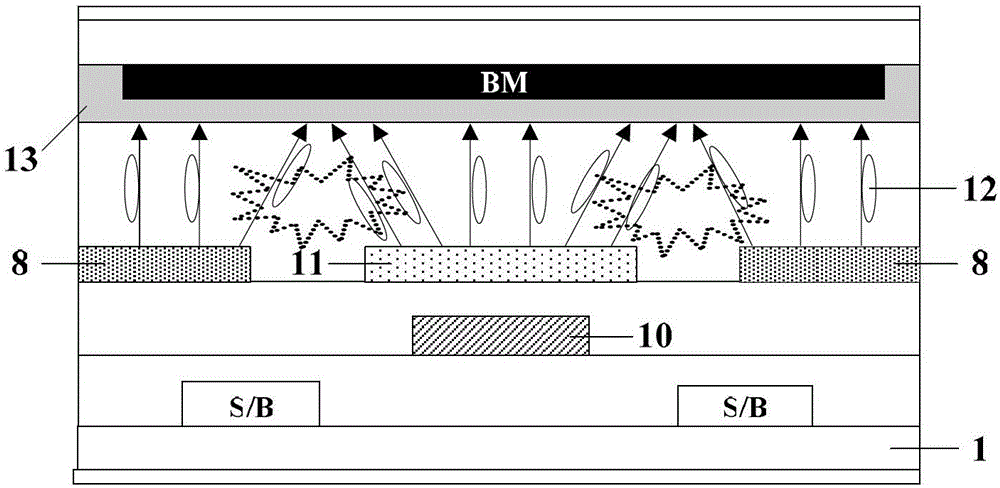
[0082] In this embodiment, the display panel adopts a normally black mode display panel, that is, when no voltage is applied to the display panel (there is no electric field or a weak electric field is formed between the pixel electrode and the common electrode), the effective display of the display panel corresponding to the liquid crystal molecules The area is opaque; when a voltage is applied (a strong electric field is formed between the pixel electrode and the common electrode), the effective display area of ​​the display panel corresponding to the liquid crystal molecules transmits light.

[0083] 1) In this embodiment, the difference between the display panel and the display panel in Embodiment 1 is that the shielding electrode in this embodiment is connected to the common electrode line, so as to ensure that the potential of the shielding electrode is equal to the potential of the common electrode.

[0084] Since the display panel in this embodiment adopts a normally bl...


PUM


Abstract

A display panel comprises an array substrate and a colour filter substrate, the array substrate comprising a plurality of data lines (10), the colour filter substrate comprising a common electrode (13), and the array substrate also comprising a shielding electrode (11) which is disposed above the plurality of data lines (10) and between which and the common electrode (13) an electric field is formed. The display panel can not only eliminate the defect that leakage of light will be generated during side-viewing or pressing, but also further reduce the width of a black matrix, thereby increasing the aperture ratio of a unit pixel.

Description

technical field [0001] The invention belongs to the technical field of display manufacturing, and in particular relates to a display panel, a method for manufacturing the display panel, and a display device including the display panel. Background technique [0002] With the development of display manufacturing technology, liquid crystal display technology has developed rapidly, and has gradually replaced traditional picture tube displays and become the mainstream of future flat panel displays. In the field of liquid crystal display technology, TFT-LCD (Thin Film Transistor Liquid Crystal Display) is widely used in televisions, computers, Mobile phones and other fields. [0003] Among them, TN (Twisted Nematic, Twisted Nematic Technology) display panel has become the most widely used entry-level LCD panel due to its low production cost, and is widely used in mainstream low-end LCD monitors on the market. [0004] The TN display panel is made by assembling an array substrate...

Claims


Application Information

Patent Timeline
Patent Type & Authority Patents(China)
IPC IPC(8): G02F1/1343G02F1/1362G02F1/1333
CPCG02F2001/136218G02F1/136209G02F1/136218
Inventor 林鸿涛封宾刘家荣
Owner BOE TECH GRP CO LTD
Why Eureka
Try Eureka