
Stereo display panel and display panel
A display panel and stereoscopic display technology, applied in the direction of electric solid-state devices, semiconductor devices, optics, etc., to achieve the effect of improving the accuracy of lamination
- Summary
- Abstract
- Description
- Claims
- Application Information
AI Technical Summary
Problems solved by technology
Method used
Image

Examples
Embodiment Construction
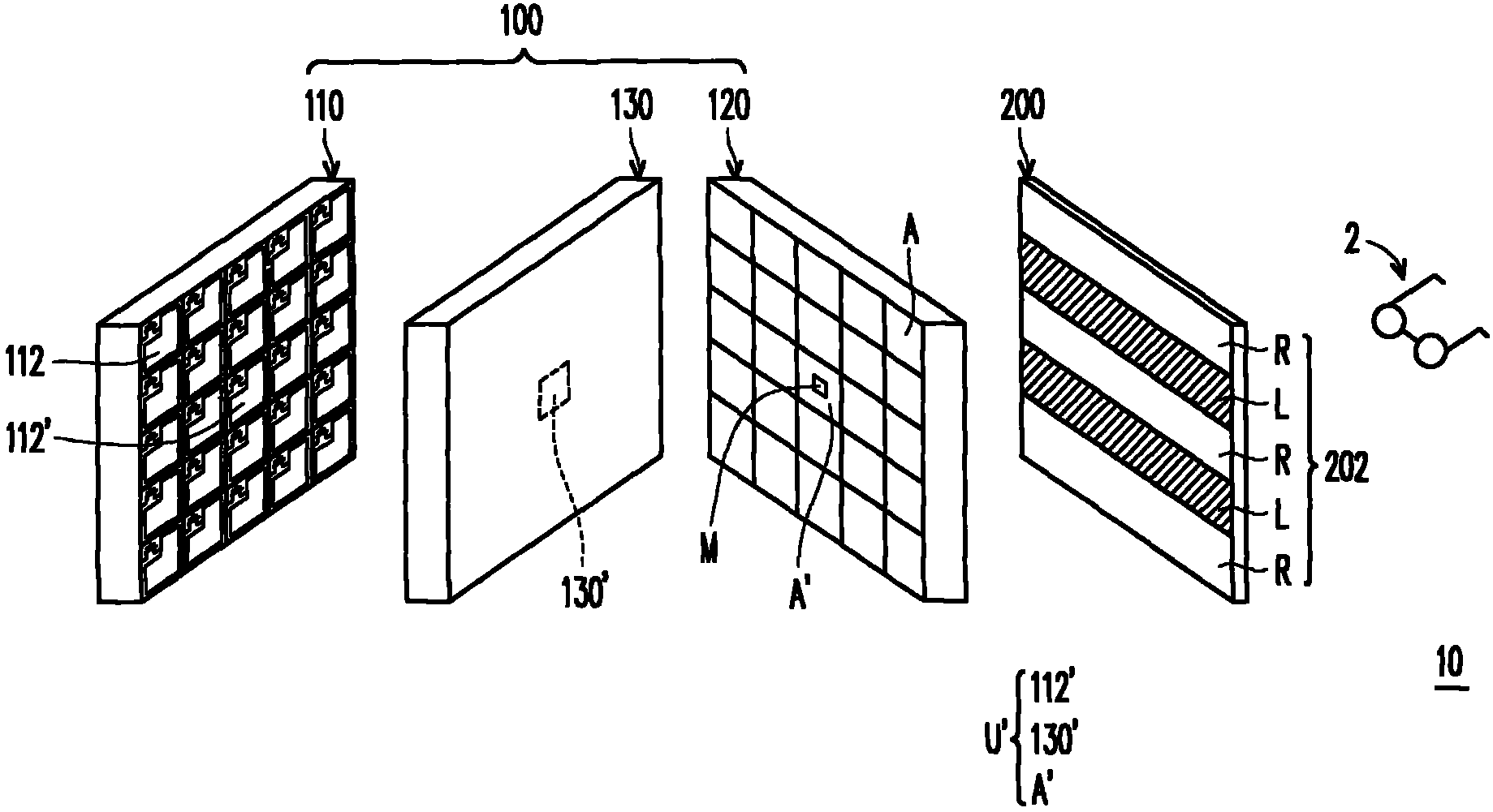
[0095] figure 1 is a three-dimensional exploded schematic diagram of the three-dimensional display panel according to the first embodiment of the present invention. Please refer to figure 1 , the three-dimensional display panel 10 includes a display panel 100 and a three-dimensional retardation film 200 . The display panel 100 includes a plurality of pixel units, and at least one of the pixel units is an alignment pixel unit U'. The display panel 100 includes a first substrate 110 , a plurality of pixel structures 112 , a second substrate 120 , a display medium 130 and at least one pair of alignment marks M. As shown in FIG. The pixel structure 110 is located on the first substrate 110 . The second substrate 120 is located opposite to the first substrate 110 . The display medium 130 is located between the first substrate 110 and the second substrate 120 . The three-dimensional retardation film 200 is disposed on the second substrate 120 .
[0096] The material of the fir...
PUM
 Abstract
Description
Claims
Application Information