Method for manufacturing touch display panel

A technology for a display panel and a manufacturing method, which is applied to static indicators, data processing input/output processes, instruments, etc., can solve the problems of increasing the thickness and weight of touch panels, and avoid the influence of high temperature and reduce the thickness and weight. , to avoid the effect of color cast

Inactive Publication Date: 2012-09-26
INNOLUX CORP +1
View PDF5 Cites 11 Cited by
  • Summary
  • Abstract
  • Description
  • Claims
  • Application Information

AI Technical Summary

Problems solved by technology

[0004] However, since the thin film transistor substrate 10 and the color filter substrate 20 each have a certain thickness, and then add the thickness of the touch panel 30 and the water glue 25, the thickness and weight of the overall touch panel increase.

Method used


Image

  • Method for manufacturing touch display panel
  • Method for manufacturing touch display panel
  • Method for manufacturing touch display panel

Examples


Embodiment Construction

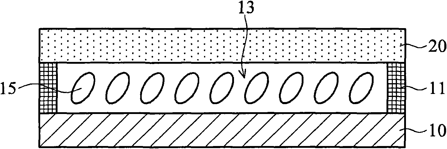
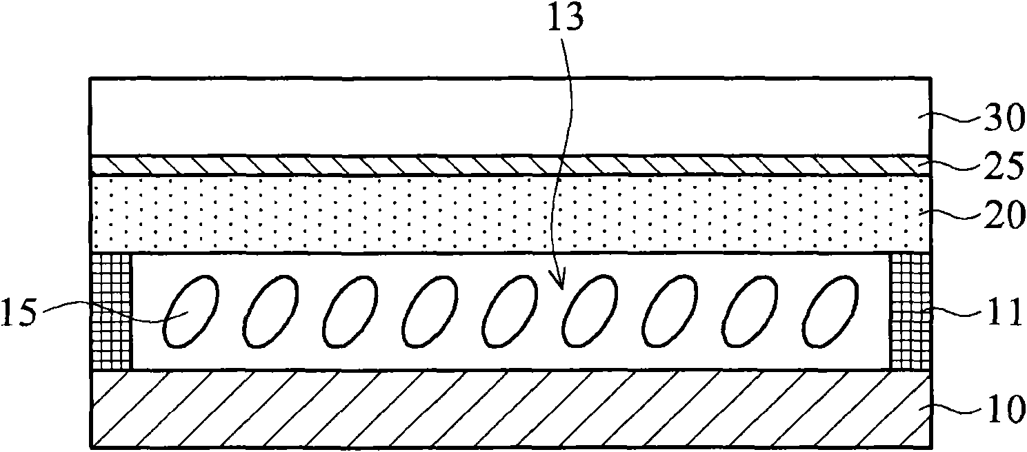
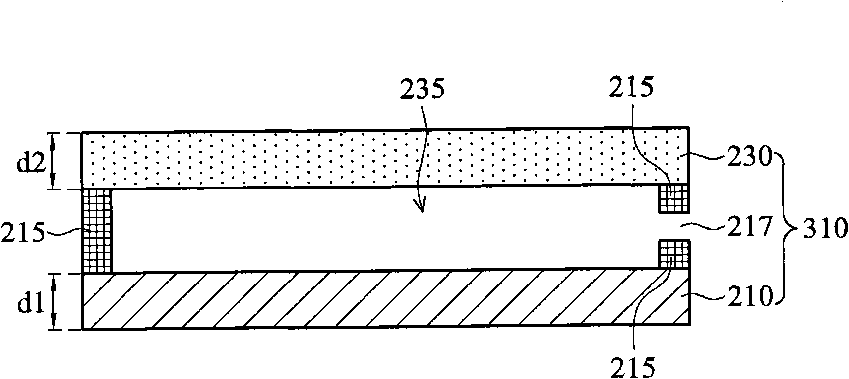
[0033] The present invention provides a method for manufacturing a touch panel, comprising the following steps: providing a display panel, wherein the display panel includes a first substrate and a second substrate oppositely arranged; thinning the a display panel; and forming a touch sensor on an outer surface of the thinned display panel. In the embodiment of the present invention, the color filter element is formed on the surface of the first substrate close to the second substrate, so the first substrate is called the color filter substrate in the embodiment of the present invention; similarly, the second substrate It is called a thin film transistor substrate. The specific implementation method is to Figures 2A-3C Take what is revealed as an example.

[0034] Figures 2A-2D A cross-sectional view showing various manufacturing stages of the touch display panel. The production method includes the following steps. First, see Figure 2A , providing a display panel 310 w...


PUM


Abstract

The invention provides a method for manufacturing a touch display panel, and aims to reduce the thickness and the weight of the touch display panel, simplify the manufacturing procedure and reduce the cost of the manufacturing procedure. The method comprises the following steps of: supplying a display panel which comprises a first substrate and a second substrate opposite to the first substrate; thinning the display panel to form a thinned display panel; and forming a touch sensor on the outer side surface of the thinned display panel.

Description

technical field [0001] The present invention relates to a display panel, and in particular to a touch-sensitive display panel and a manufacturing method thereof. Background technique [0002] With the rapid advancement of science and technology, the application of consumer electronic products is becoming more and more diversified. Among many current electronic products, in addition to being light, thin, short and small, many portable electronic products (such as personal Personal digital assistants (personal digital assistants (PDAs) or mobile phones) have widely used touch panels. [0003] In a traditional touch display panel, the touch panel and the display panel are manufactured separately, and then the touch panel and the display panel are assembled together. Figures 1A-1B A cross-sectional view showing a known manufacturing method of a touch-sensitive display panel, in Figure 1A In the process, firstly, with the aid of a sealant 11, the thin film transistor substrate...

Claims


Application Information

Patent Timeline
Patent Type & Authority Applications(China)
IPC IPC(8): G06F3/041G02F1/133
Inventor 陈新立陈弘育杨秋莲彭家鹏丁景隆
Owner INNOLUX CORP
Why Eureka
Try Eureka