Display device and electronic apparatus

A technology for display devices and display areas, applied in static indicators, nonlinear optics, instruments, etc., can solve problems such as disconnection, degradation of substrates and display layers, and decrease in reliability of display devices, and achieve the effect of improving reliability

A technology for display devices and display areas, applied in static indicators, nonlinear optics, instruments, etc., can solve problems such as disconnection, degradation of substrates and display layers, and decrease in reliability of display devices, and achieve the effect of improving reliability

CN102736347AActive Publication Date: 2012-10-17SONY CORP

Image

  • Display device and electronic apparatus
  • Display device and electronic apparatus
  • Display device and electronic apparatus

Examples


Embodiment approach

[0028] A display device with an L-shaped auxiliary board portion protruding from one side of the periphery of the main board portion

[0029] 2. Variation 1

[0030] A display device with an L-shaped auxiliary board portion protruding from the peripheral corner of the main board portion

[0031] 3. Variation 2

[0032] Display device with rectangular periphery of whole substrate

[0033] 4. Application examples

[0034]

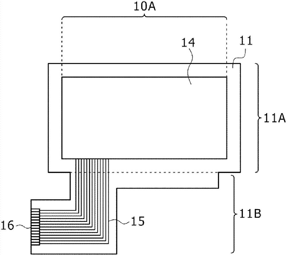
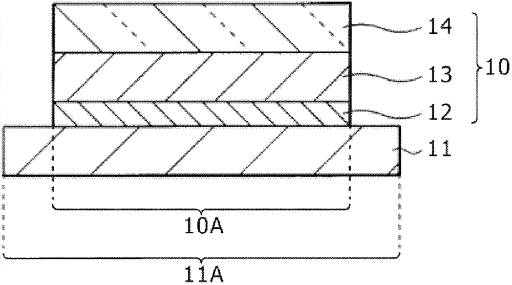
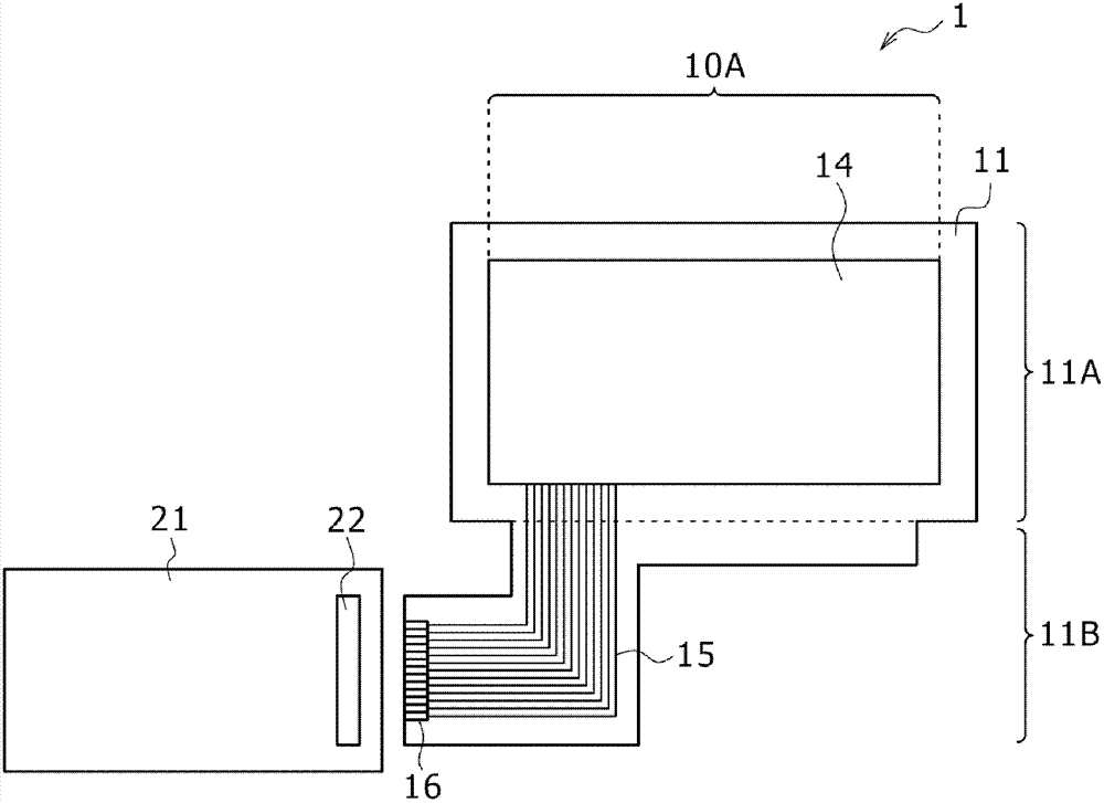
[0035] figure 1 The plane arrangement of the substrate (substrate 11) of the display device (display device 1) according to one embodiment of the present invention is shown. The display device 1 has a main board portion 11A and an auxiliary board portion 11B integrated with the main board portion 11A, and such as figure 2 As shown, the display panel 10 is arranged in the display area 10A of the main board part 11A. The display panel 10 is obtained by stacking a substrate 11, a thin film transistor (TFT) layer 12, a display layer 13, and a transparent substrate 14 in ...


PUM


Abstract

Disclosed herein is a display device including a main board part configured to have a display area including drive wiring and have a display panel disposed in the display area; and an auxiliary board part configured to be monolithic with the main board part and have extraction wiring from the drive wiring.

Description

[0001] Cross references to related applications [0002] This application contains the related subject matter disclosed in Japanese Patent Application JP2011-084731 filed with the Japan Patent Office on April 6, 2011 and claims the priority thereof, and the entire contents of which are incorporated herein by reference. Technical field [0003] The present invention relates to a display device that performs display by inputting a signal from the outside to a drive wiring of a display area, and an electronic device including the display device. Background technique [0004] In flat panel display devices such as liquid crystal display devices and electrophoretic display devices, a wiring board for inputting signals from the outside is connected to the display panel. This signal is supplied to the drive wiring of the display panel via the wiring board. The display panel is configured to include a substrate and a display layer arranged on the central portion of the substrate, and the wi...

Claims


Application Information

Patent Timeline
17 Oct 2012
Publication
CN102736347A
IPC
G02F1/167; G09G3/34
CPC
G02F1/167; G09G3/34; G02F1/13452
Inventors
铃木政人; 西正太