Tactile stimulation apparatus having a composite section comprising a semiconducting material

A stimulation device and semiconductor technology, applied in signal devices, tactile transmission signal systems, teaching aids, etc., can solve problems such as thick insulating materials, users encountering electric shocks, and insufficient insulation.

Active Publication Date: 2012-10-17
PIXART IMAGING INC
View PDF3 Cites 15 Cited by
  • Summary
  • Abstract
  • Description
  • Claims
  • Application Information

AI Technical Summary

Problems solved by technology

For example, when a user touches a specific part of a computer or other device, the user may receive an electric shock if the part is leaking electricity or is not adequately insulated
Also, some insulating materials used to cover parts of the equipment to prevent electric shock or for other purposes can be very thick

Method used


Image

  • Tactile stimulation apparatus having a composite section comprising a semiconducting material
  • Tactile stimulation apparatus having a composite section comprising a semiconducting material
  • Tactile stimulation apparatus having a composite section comprising a semiconducting material

Examples


Embodiment Construction

[0024] The following description and drawings set forth specific embodiments sufficient to enable those skilled in the art to practice the invention. Other embodiments may incorporate structural, logical, electrical, process, and other changes. The examples merely represent possible variations. Individual components and functions are optional unless explicitly required, and the order of operations may vary. Portions and features of some embodiments may be included in, or substituted for, features of other embodiments. Embodiments of the invention set forth in the claims encompass all available equivalents of those claims. In the embodiments of the present invention, the term "invention" mentioned here, which may be individually or collectively, is only for convenience of expression, and is not intended to limit the scope of the application to any single invention or inventive concept. Many inventions.

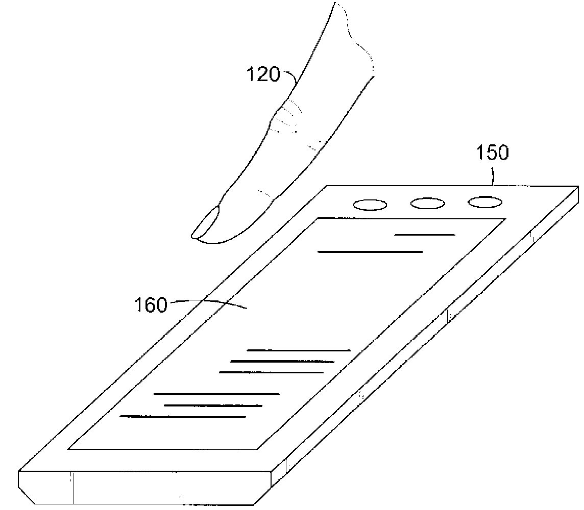
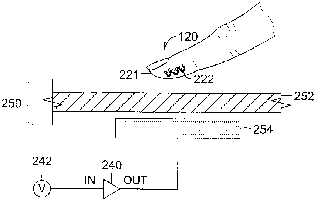
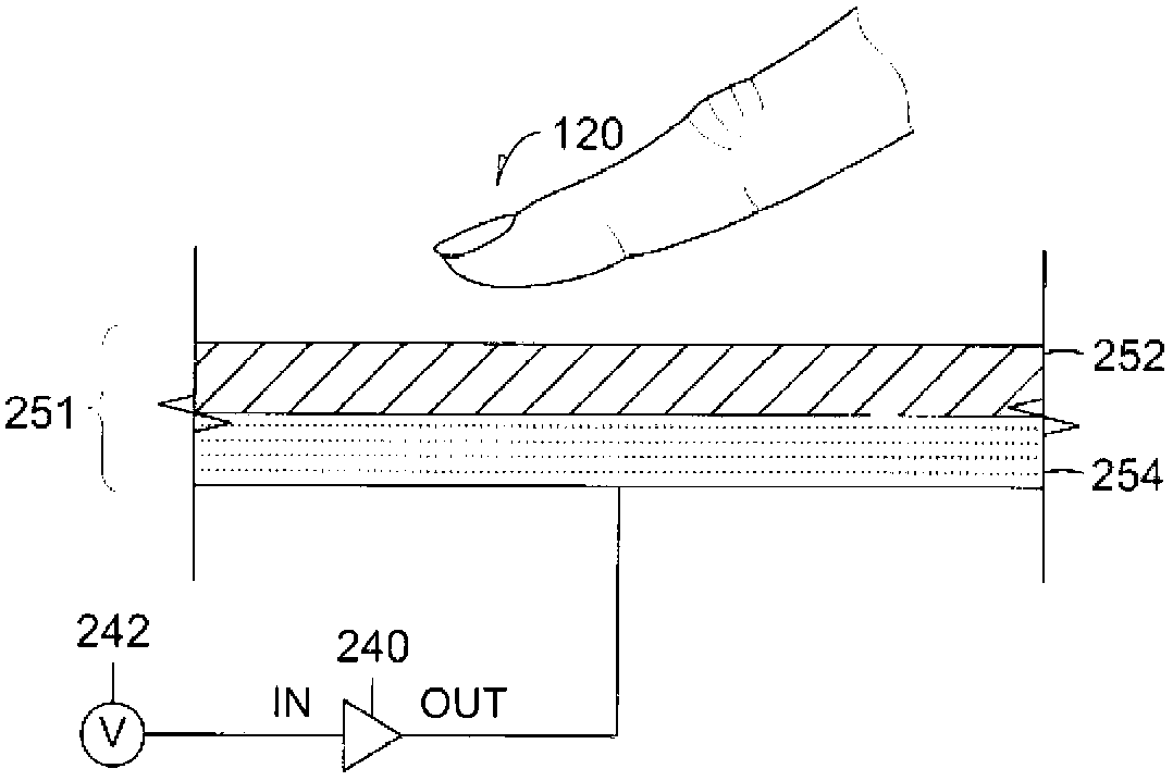
[0025] figure 1 A schematic diagram of an example of a tactile stimul...


PUM


Abstract

Embodiments of tactile stimulation apparatuses and components of such apparatuses are generally described herein. For example, in one embodiment, a tactile stimulation apparatus is provided. This tactile stimulation apparatus has a composite section comprising an insulation region and a semiconducting region that is proximate to the insulation region. This insulation region is touchable by a body member. Additionally included is a voltage source proximate to the semiconducting region. Here, the voltage source is configured to charge the semiconducting region to an electric potential, which produces an electrosensory sensation on the body member.

Description

[0001] Cross References to Related Applications [0002] This application claims the benefit of U.S. Application No. 12 / 793,563, filed June 3, 2010, entitled "Tactile Stimulation Device Having Composite Sections Including Semiconductor Materials," and U.S. Patent Application No. Provisional Application No. 61 / 260,554, entitled "Interface Apparatus for Touch Input," is the priority of the patent application, the disclosure of which is incorporated herein by reference. Background technique [0003] Shock can occur when an electric current suddenly flows through a part of the body, typically causing irritation of a nerve. For example, a user may experience an electric shock when touching a particular part of a computer or other device if that part is leaking electricity or is not adequately insulated. Additionally, some insulating materials used to cover parts of the equipment may be very thick for protection against electric shock or for other purposes. The thickness of the in...

Claims


Application Information

Patent Timeline
Patent Type & Authority Applications(China)
IPC IPC(8): G06F3/041G09B21/00H03K17/96
CPCG08B6/00H03K2217/96062G06F3/0414G09B21/003G06F3/016G06F3/044H03K2217/96031H03K17/9622G06F3/0443G06F3/0412
Inventor V·马基宁J·琳加玛Z·盖尔扎
Owner PIXART IMAGING INC
Why Eureka
Try Eureka