

A kind of igbt with terminal deep level impurity layer
A deep-level impurity and terminal technology, which is applied in the direction of electrical components, circuits, semiconductor devices, etc., can solve the problems of device avalanche breakdown, large conduction loss, and small conduction voltage drop, so as to improve the turn-off characteristics of the device, Effect of reducing high-temperature leakage current and improving shutdown characteristics
- Summary
- Abstract
- Description
- Claims
- Application Information
AI Technical Summary
Problems solved by technology
Method used
Image

Examples
Embodiment Construction
[0020] Specific implementation plan
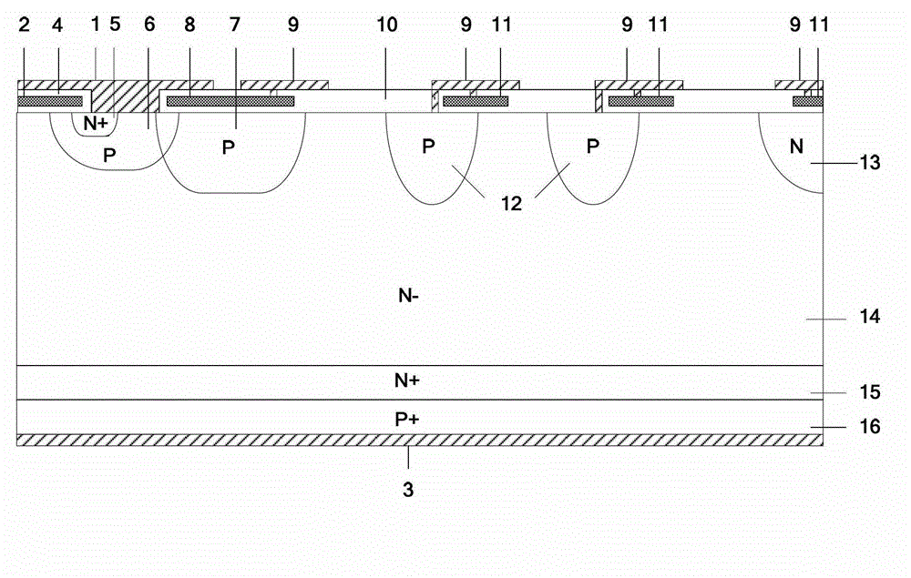
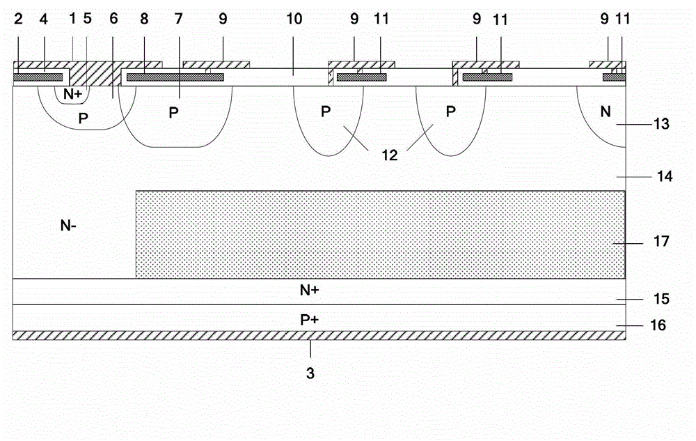
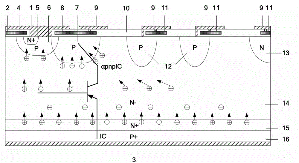
[0021] An IGBT with a terminal deep-level impurity layer, and its cell structure is as figure 2 As shown, it includes a metal active emitter 1, a polysilicon gate electrode 2, a metal collector 3, a gate oxide layer 4, an N+ active region 5, a P-type base region 6, a P-type equipotential ring 7, a polysilicon field plate 8, Metal aluminum field plate 9, terminal region oxide layer 10, terminal polysilicon field plate 11, P-type field limiting ring 12, N+ electric field stop ring 13, N- drift region 14, N+ electric field termination layer 15, P+ collector region 16;
[0022] The device from the bottom layer to the top is the metal collector 3, the P+ collector region 16, the N+ electric field stop layer 15, and the N- drift region 14. The P-type base region 6 is located on the top of the N- drift region 14, and the P-type base region 6 has N+ active area 5, the cell surface is in contact with the N+ active area 5 and the P-type base area 6 resp...
PUM
 Abstract
Description
Claims
Application Information