Double poly-crystal plane strain BiCMOS integrated device based on SOI (Silicon On Insulator) substrate and preparation method

A plane strain, integrated device technology, applied in semiconductor/solid-state device manufacturing, electric solid-state devices, semiconductor devices, etc., can solve the problems of low mechanical strength, high cost, incompatibility with wide application and development, etc.

Inactive Publication Date: 2015-04-22
XIDIAN UNIV
View PDF5 Cites 0 Cited by
  • Summary
  • Abstract
  • Description
  • Claims
  • Application Information

AI Technical Summary

Problems solved by technology

Although GaAs and InP-based compound devices have superior frequency characteristics, their preparation process is more complicated than Si process, high cost, difficult to prepare large-diameter single crystal, low mechanical strength, poor heat dissipation performance, incompatibility with Si process and lack of SiO 2 Such passivation layer and other factors limit its wide application and development.

Method used


Image

  • Double poly-crystal plane strain BiCMOS integrated device based on SOI (Silicon On Insulator) substrate and preparation method

Examples


Embodiment 1

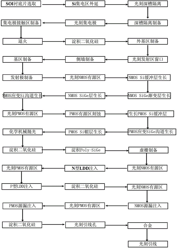
[0111] Embodiment 1: A self-aligned process is used to prepare a dual-polycrystalline plane-strain BiCMOS integrated device and circuit based on an SOI substrate with a conductive channel of 22nm. The specific steps are as follows:

[0112] Step 1, epitaxial growth.

[0113] (1a) Select the SOI substrate, the support material of the lower layer of the substrate is Si, and the middle layer is SiO 2 , with a thickness of 150nm, and the upper material is doped with a concentration of 1×10 16 cm -3 N-type Si with a thickness of 100nm;

[0114] (1b) Using the chemical vapor deposition (CVD) method, at 600 ° C, grow a layer of N-type epitaxial Si layer with a thickness of 50 nm on the upper Si material, as the collector region, and the doping concentration of this layer is 1× 10 16 cm -3 .

[0115] Step 2, isolation area preparation.

[0116] (2a) Deposit a layer of SiO with a thickness of 300nm on the surface of the epitaxial Si layer at 600°C by chemical vapor deposition (C...

Embodiment 2

[0169] Embodiment 2: A self-aligned process is used to prepare a dual-polycrystalline plane-strain BiCMOS integrated device and circuit based on an SOI substrate with a conductive channel of 30 nm. The specific steps are as follows:

[0170] Step 1, epitaxial growth.

[0171] (1a) Select the SOI substrate, the support material of the lower layer of the substrate is Si, and the middle layer is SiO 2 , with a thickness of 300nm, and the upper material is doped with a concentration of 5×10 16 cm -3 N-type Si with a thickness of 120nm;

[0172] (1b) Using chemical vapor deposition (CVD), grow an N-type epitaxial Si layer with a thickness of 80nm on the upper Si material at 700°C as the collector region, and the doping concentration of this layer is 5× 10 16 cm -3 .

[0173] Step 2, isolation area preparation.

[0174] (2a) Deposit a layer of SiO with a thickness of 400nm on the surface of the epitaxial Si layer at 700°C by chemical vapor deposition (CVD). 2 Floor;

[0175...

Embodiment 3

[0227] Embodiment 3: A dual-polycrystalline plane-strain BiCMOS integrated device and circuit based on an SOI substrate with a conductive channel of 45nm prepared by a self-alignment process, the specific steps are as follows:

[0228] Step 1, epitaxial growth.

[0229] (1a) Select the SOI substrate, the support material of the lower layer of the substrate is Si, and the middle layer is SiO 2 , with a thickness of 400nm, and the upper material is doped with a concentration of 1×10 17 cm -3 N-type Si with a thickness of 150nm;

[0230] (1b) Using the method of chemical vapor deposition (CVD), grow a layer of N-type epitaxial Si layer with a thickness of 100nm on the upper layer of Si material at 750°C, as the collector region, and the doping concentration of this layer is 1× 10 17 cm -3 .

[0231] Step 2, the implementation method of isolation area preparation is:

[0232] (2a) Deposit a layer of SiO with a thickness of 500nm on the surface of the epitaxial Si layer at 8...


PUM


Abstract

The invention discloses a double poly-crystal plane strain BiCMOS integrated device based on a SOI (Silicon On Insulator) substrate and a preparation method. The preparation method comprises the following steps: preparing a deep slot isolator on the SOI substrate; forming a collector contact region, a nitride side wall and a base region window; growing SiGe and Poly-Si on the base region, thereby forming a SiGe HBT (Heterojunction Bipolar Transistor) device; etching a slot on a NMOS (N-channel Metal Oxide Semiconductor) device active region, preparing a grid dielectric layer and a grid poly-crystal on the NMOS device active region, thereby forming a NMOS device; etching a slot on a PMOS (P-channel Metal Oxide Semiconductor) device active region and preparing a drain and a grid on the PMOS device active region, thereby forming a PMOS device; and photo-etching a lead, thereby preparing a BiCMOS integrated device and a circuit. According to the preparation method, a BiCMOS integrated circuit with an enhanced property is prepared by adopting a self-aligning technology and fully utilizing the characteristics that the electronic mobility of a spreading strain Si material is higher than that of a semiconductor Si material and the hole mobility of a compressive strain SiGe material is higher than that of the semiconductor Si material.

Description

technical field [0001] The invention belongs to the technical field of semiconductor integrated circuits, and in particular relates to the preparation of a double polycrystalline plane strain BiCMOS integrated device based on an SOI substrate by a self-alignment process and a preparation method. Background technique [0002] The integrated circuit is the cornerstone and core of the economic development of the information society. Just as the American engineering and technical circles recently named the fifth electronic technology among the world's 20 greatest engineering technological achievements in the 20th century, "From vacuum tubes to semiconductors and integrated circuits, everything has It has become the cornerstone of intelligent work in various industries in the contemporary era." The integrated circuit is one of the typical products that can best reflect the characteristics of the knowledge economy; at present, the electronic information industry based on the integr...

Claims


Application Information

Patent Timeline
Patent Type & Authority Patents(China)
IPC IPC(8): H01L27/12H01L21/84
Inventor 张鹤鸣王斌宣荣喜胡辉勇宋建军吕懿舒斌郝跃
Owner XIDIAN UNIV
Why Eureka
Try Eureka