Key device and light guide member layer

A technology of light guide film and optical film layer, which is applied in electrical components, electrical switches, circuits, etc., can solve the problems of increasing the thickness of buttons, unfavorable thin-shaped design of electronic products, etc., so as to reduce the thickness and avoid the mutual influence of electrical signals. , the effect of reducing production costs

Inactive Publication Date: 2012-12-19
HONG FU JIN PRECISION IND (SHENZHEN) CO LTD +1
View PDF4 Cites 42 Cited by
  • Summary
  • Abstract
  • Description
  • Claims
  • Application Information

AI Technical Summary

Problems solved by technology

[0003] The button device with the above structure, because a rubber layer is added between the button layer and the light guide layer, this increases the thickness of the entire button, which is not conducive to the thin design of electronic products

Method used


Image

  • Key device and light guide member layer
  • Key device and light guide member layer
  • Key device and light guide member layer

Examples


Embodiment Construction

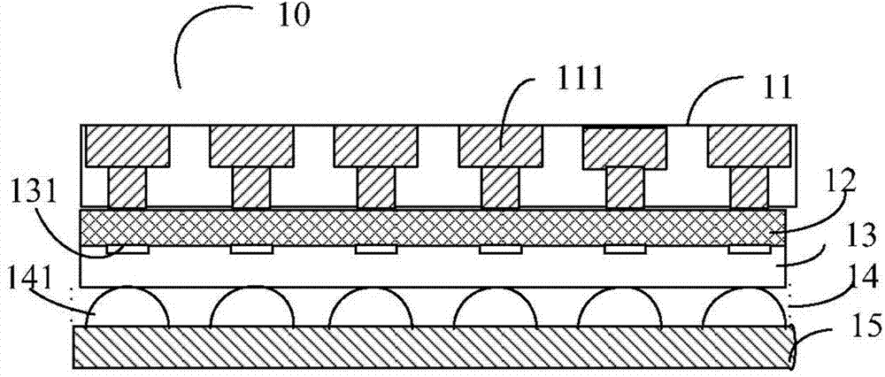
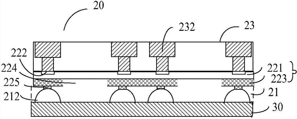
[0017] see figure 2 , which is a cross-sectional view of the key device 20 in an embodiment of the present invention. The button device 20 can be installed on a circuit board equipped with a corresponding button circuit, and the button device 20 can be used to realize the conduction and isolation between each button and the circuit on the circuit board, so as to realize the button input operation. The button device 20 includes a circuit board 30 , a dome layer 21 , a light guide film layer 22 and a button layer 23 from bottom to top.

[0018] The dome layer 21 includes a plurality of domes 212 made of metal material disposed on the circuit board 30 . The button layer 23 includes several buttons 232 . The button 232 can be made of silica gel, and characters and symbols such as Chinese, English, or Japanese are printed on its surface, and each button corresponds to a dome 212 .

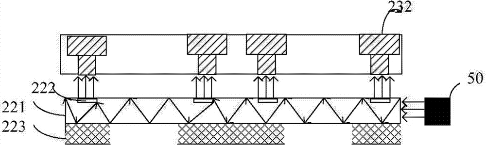
[0019] The light guiding film layer 22 includes an optical film layer 221 and a rubber layer 223...


PUM


Abstract

The invention relates to a light guide membrane layer for a key device. The light guide membrane layer comprises an optical membrane layer and a rubber layer arranged on one side of the optical membrane layer and formed with the optical membrane layer to a whole, wherein at least one accommodating region is formed on the rubber layer. In addition, the invention also provides a key device which comprises a key layer, a metal dome switch layer and a light guide membrane layer arranged between the key layer and the metal dome switch layer, the light guide membrane layer comprises the optical membrane layer and the rubber formed with the optical membrane layer to a whole, and at least one accommodating region is formed on the rubber layer. According to the invention, the optical membrane layer and the rubber layer are formed into a whole, so that the thickness of the whole key structure is lowered; and meanwhile the accommodating region is formed on the rubber layer, a larger accommodating space is gained for elements in the accommodating region, mutual influences of electrical signals between the key and the elements in the accommodating region is avoided, and the production cost can be lowered.

Description

technical field [0001] The invention relates to the technical field of keys for electronic products, in particular to a key device and a light guide film layer thereof. Background technique [0002] In the button design of electronic products such as mobile phones, in order to make it usable in the dark, lighting settings are used for the buttons, and LEDs are generally used as light sources. In order to reduce the number of LEDs and reduce costs, a light guide film is often used to transmit the light to make the light more uniform. Such as figure 1 As shown, the traditional mobile phone button 10 with a light guide film includes a button layer 11, a rubber layer 12, a light guide film layer 13, a dome layer (dome) 14, a circuit board 15 and a button layer that are stacked from top to bottom. LEDs on the circuit board (not shown). The button layer 11 includes several buttons 111, the rubber layer 12 is made of transparent or translucent material, the light guide film laye...

Claims


Application Information

Patent Timeline
Patent Type & Authority Applications(China)
IPC IPC(8): H01H13/83
Inventor 欧阳国祥
Owner HONG FU JIN PRECISION IND (SHENZHEN) CO LTD
Why Eureka
Try Eureka