Switch circuit capable of quickly discharging transistor parasitic capacitance charge and charge discharging method thereof

A technology of parasitic capacitance and switching circuit, which is applied in the field of switching control circuit, can solve the problem of 2 times the delay time ratio damage, etc., and achieve the effect of reducing time overhead, reducing load start-up delay time, and eliminating delay phenomenon

Active Publication Date: 2012-12-19
SUZHOU YONGJIAN PHOTOELECTRIC TECH
View PDF1 Cites 9 Cited by
  • Summary
  • Abstract
  • Description
  • Claims
  • Application Information

AI Technical Summary

Problems solved by technology

V G The pulse width is only 20ns to display a certain level of grayscale, and the brightness is doubled by using twice the pulse width of 20ns to display the grayscale, but the existence of the delay time not only destroys the ratio of 2 times, but also causes the actual lighting of the 20ns pulse width The time is not 20ns
And do not see the public report about the solution of this problem at present, therefore urgently need a kind of technology to solve this difficult problem

Method used


Image

  • Switch circuit capable of quickly discharging transistor parasitic capacitance charge and charge discharging method thereof
  • Switch circuit capable of quickly discharging transistor parasitic capacitance charge and charge discharging method thereof
  • Switch circuit capable of quickly discharging transistor parasitic capacitance charge and charge discharging method thereof

Examples


Embodiment 1

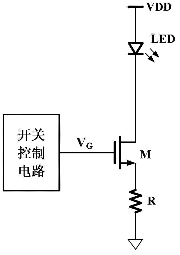
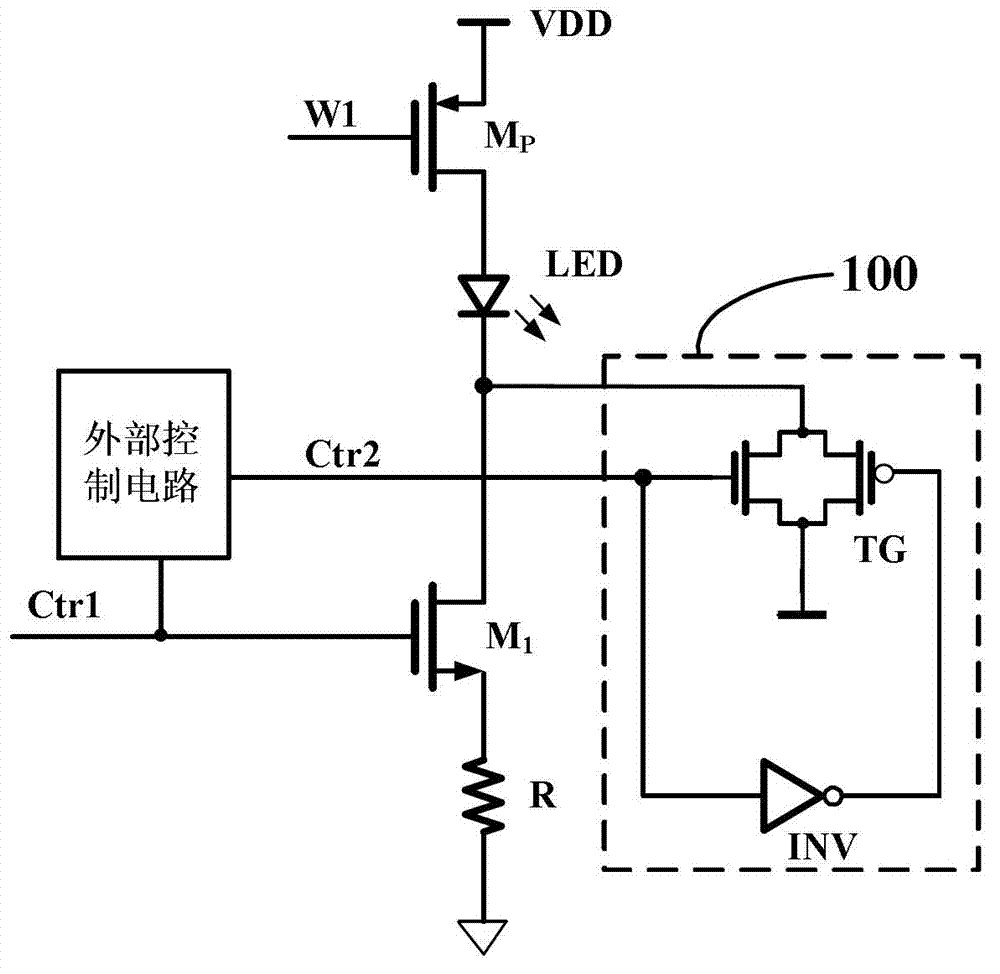
[0049] Such as figure 2 As shown, a switch circuit with a fast discharge transistor parasitic capacitance charge, including: NMOS tube M connected to the LED 1 , a resistor R and a charge discharge circuit 100 .

[0050] NMOS tube M 1 The drain of the LED is connected to the cathode of the LED and the input end of the charge discharge circuit 100, and the anode of the LED is connected through the PMOS transistor M p Connect to supply voltage V DD , NMOS tube M 1 The source of the resistor R is connected to one end of the resistor R, the other end of the resistor R is grounded, and the output terminal of the charge discharge circuit 100 is connected to a reference potential;

[0051] NMOS tube M 1 The gate of the gate receives the control signal Ctr1 provided by the external device, and the external control circuit provides the control signal Ctr2 to the control terminal of the charge discharge circuit 100 according to the state of the control signal Ctr1.

[0052] The c...

Embodiment 2

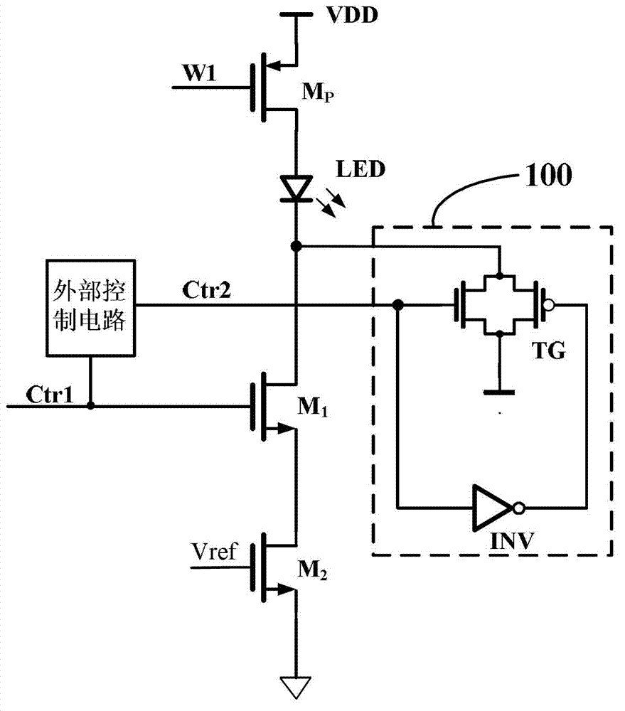
[0056] Such as image 3 As shown, a switch circuit with a fast discharge transistor parasitic capacitance charge, including: NMOS tube M connected to the LED 1 , NMOS tube M 2 and the charge discharge circuit 100.

[0057] NMOS tube M 1 The drain of the LED is connected to the cathode of the LED and the input end of the charge discharge circuit 100, and the anode of the LED is connected through the PMOS transistor M p connected to supply voltage V DD , NMOS tube M 1 The source and NMOS tube M 2 The drain is connected, the NMOS transistor M 2 The source of the charge discharge circuit 100 is connected to the reference potential, and the NMOS transistor M 2 The gate receives a given reference voltage signal V ref ;

[0058] NMOS tube M 1 The gate of the gate receives the control signal Ctr1 provided by the external device, and the external control circuit provides the control signal Ctr2 to the control terminal of the charge discharge circuit 100 according to the state...

Embodiment 3

[0063] Such as Figure 4 As shown, a switch circuit with a fast discharge transistor parasitic capacitance charge, including: NMOS tube M connected to the LED 1 and the charge discharge circuit 100.

[0064] NMOS tube M 1 The drain of the LED is connected to the cathode of the LED and the input end of the charge discharge circuit 100, and the anode of the LED is connected through the PMOS transistor M p Connect to supply voltage V DD , NMOS tube M 1 The source of the charge discharge circuit 100 is connected to the reference potential;

[0065] NMOS tube M 1 The gate of the gate receives the control signal Ctr1 provided by the external device, and the external control circuit provides the control signal Ctr2 to the control terminal of the charge discharge circuit 100 according to the control signal Ctr1.

[0066] The charge discharge circuit 100 is composed of an NMOS transistor M N Composition; M N The drain of is the input end of the charge discharge circuit 100, M ...


PUM


Abstract

The invention claims a switch circuit capable of quickly discharging transistor parasitic capacitance charge. The switch circuit comprises a transistor connected with the load; the input end of the transistor is connected with a charge discharging circuit; the charge discharging circuit receives a second controlling signal provided by the external device for discharging the charge on the transistor parasitic capacitance under the action of the second controlling signal, and lowering the potential on the input end of the transistor to the reference potential. At the same time, the invention also discloses the charge discharging method of the switch circuit. The switch circuit provided by the invention can effectively eliminate the delay phenomenon when starting up the load through quickly regulating the potential on the input end of the transistor down by utilizing the charge discharging circuit in the transitional stage of turning from on to off, thus greatly reducing the time cost wasted on reducing the virtual high potential of the input end after the transistor is on.

Description

technical field [0001] The invention belongs to the technical field of switch control circuits, and in particular relates to a switch circuit with a fast discharge transistor parasitic capacitance charge and a charge discharge method thereof. Background technique [0002] In the application of using MOS tubes as adjustment and control switches, one end of an electronic component (including but not limited to resistors, transistors, LEDs, etc.) is often connected to a switch circuit (such as a MOS tube), and the switch circuit is used as an electronic component A circuit structure in which a device switches to control or conduct electric current. Although in theory turning on the MOS tube can make the electronic components connected to the MOS tube conduct normally, but in practice, the MOS tube itself is already in the conducting state, but there is no current or current in the electronic components connected to it. Too small, it takes a certain amount of time for the curre...

Claims


Application Information

Patent Timeline
Patent Type & Authority Applications(China)
IPC IPC(8): H02M1/36H02M1/32
Inventor 赵一尘卢晓冬何乐年
Owner SUZHOU YONGJIAN PHOTOELECTRIC TECH
Why Eureka
Try Eureka