Multi-version code stream storage circuit architecture for configuration memory dedicated for FPGA (Field Programmable Gate Array)
A storage circuit and memory technology, applied in the field of integrated circuits, to achieve stable remote update, improve debugging and testing efficiency
- Summary
- Abstract
- Description
- Claims
- Application Information
AI Technical Summary
Problems solved by technology
Method used
Image
Examples
Embodiment Construction
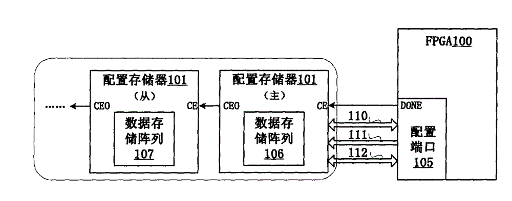
[0031] figure 1 It is a schematic diagram of the cascaded application configuration interface of the FPGA device and the configuration memory 101. Here, in order to illustrate the configuration principle of the FPGA100 device and the cascadable characteristics of the configuration memory 101, only the interface signals related to the configuration and cascade characteristics are marked out. , mainly includes: control enable signal CE, control enable output signal CEO and FPGA configuration port 105; FPGA configuration port 105 mainly includes: configuration completion signal DONE, control bus 110, address bus 111 and data bus 112.
[0032] For the configuration of the FPGA100 device, it is necessary to connect the configuration completion signal DONE of the FPGA100 device with the control enable signal CE of the configuration memory 101 (main); 111 sends address information to the configuration memory 101 (master), and interacts with the configuration memory 101 (master) throu...
PUM
 Abstract
Description
Claims
Application Information


