Touch panel integrated display device and method for manufacturing same

A touch panel and display device technology, applied in the direction of static indicators, electric solid devices, semiconductor devices, etc., can solve the problems of increased manufacturing cost and increased material cost, and achieve the simplification of the manufacturing process and the suppression of light transmission Effect of reducing and preventing deterioration of S/N ratio

Inactive Publication Date: 2013-01-16
ALPS ALPINE CO LTD
View PDF10 Cites 13 Cited by
  • Summary
  • Abstract
  • Description
  • Claims
  • Application Information

AI Technical Summary

Problems solved by technology

Therefore, a heat treatment process is added, resulting in an increase in manufacturing cost
In addition, high heat resistance is required as a transparent base material for touch panels, so there are restrictions on the materials that can be used as base materials, which in turn leads to an increase in material costs

Method used


Image

  • Touch panel integrated display device and method for manufacturing same
  • Touch panel integrated display device and method for manufacturing same
  • Touch panel integrated display device and method for manufacturing same

Examples


no. 1 approach

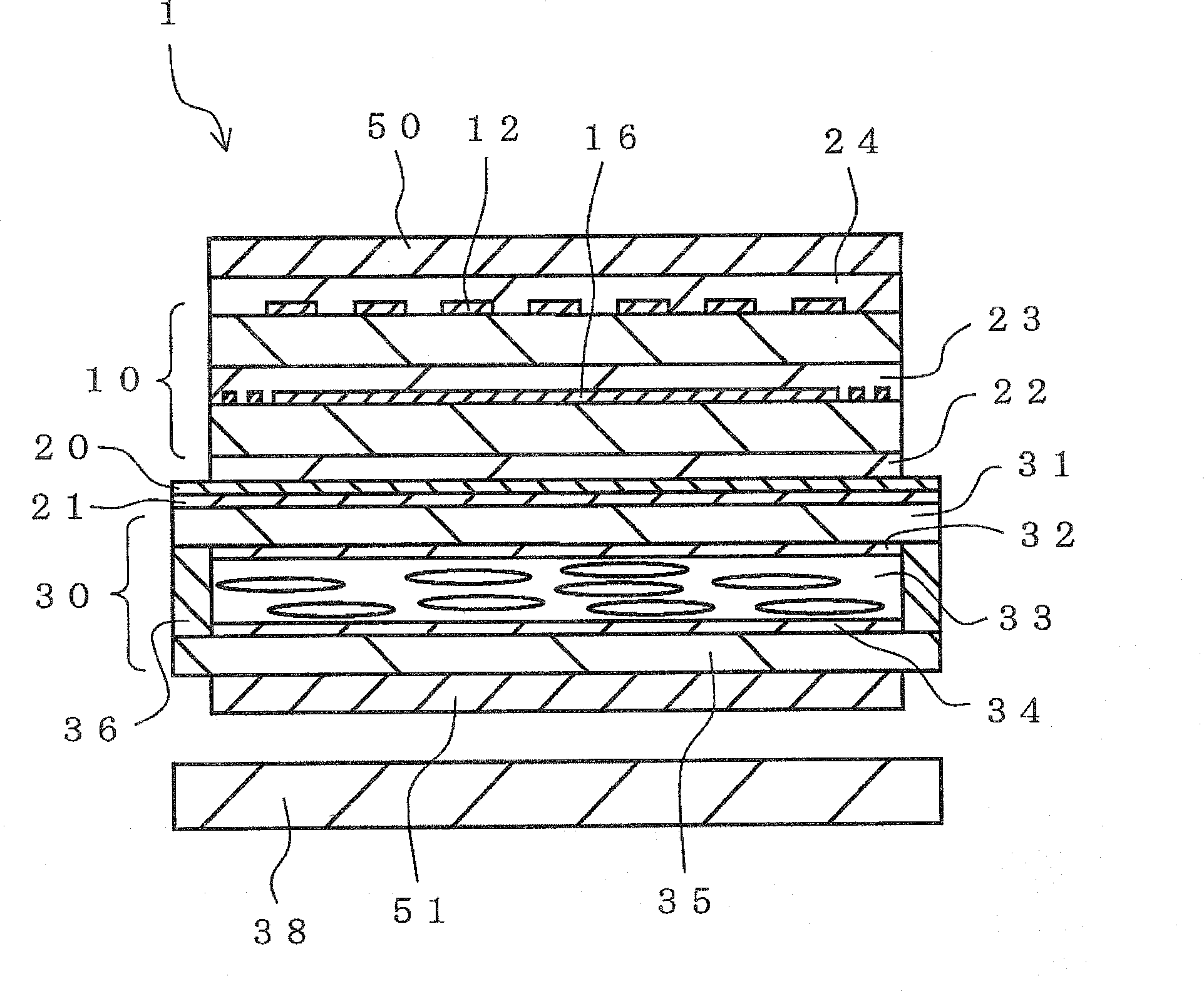
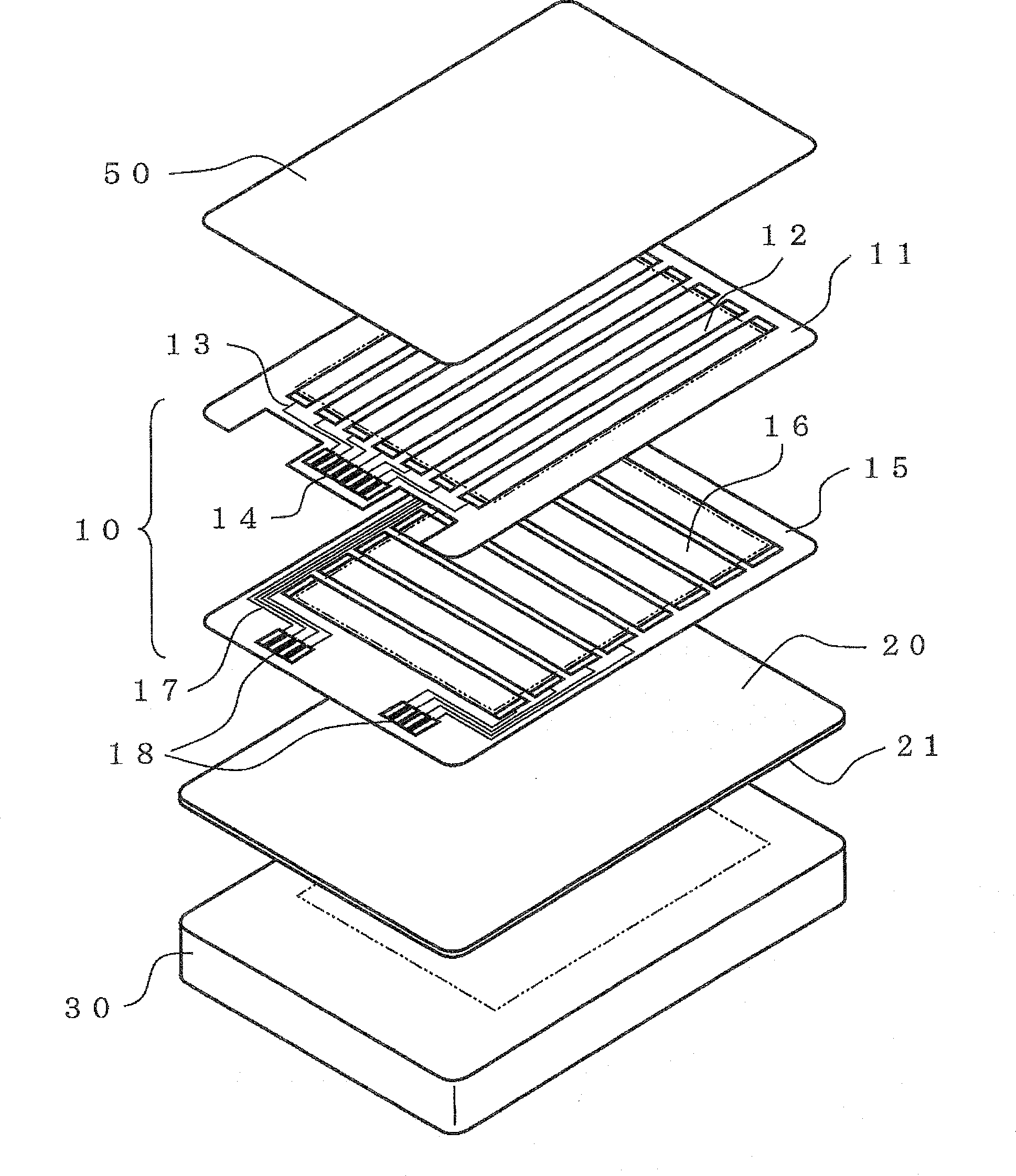
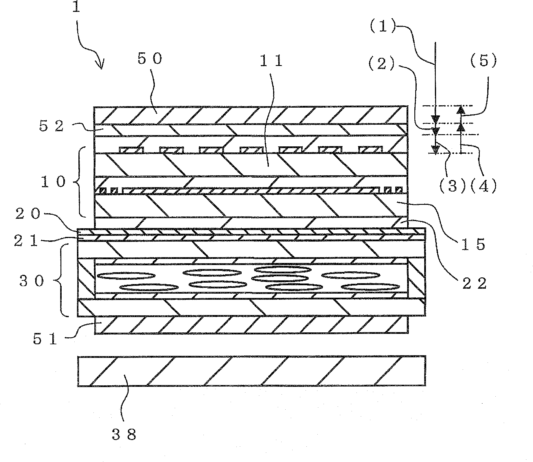
[0085] figure 1 A cross-sectional view showing the touch-panel-integrated display device 1 of the first embodiment. figure 2 An exploded perspective view of the touch panel integrated display device 1 is shown. In addition, in each drawing, the dimension is changed suitably and shown for convenience of observation.

[0086] like figure 1 As shown, in the touch-panel-integrated display device 1 of this embodiment, a liquid crystal panel 30 is used as a display panel for displaying images and text information, and a light-transmissive touch panel is arranged on the display surface side of the liquid crystal panel 30 . The capacitive touch panel 10 of the panel. The operator can visually recognize the image from the liquid crystal panel 30 through the capacitive touch panel 10 , and can perform an input operation through the touch panel 10 while viewing a displayed image, a menu display, and the like.

[0087] On the display surface side of the liquid crystal panel 30 , th...

no. 2 approach

[0117] Figure 5 It is a cross-sectional view of a touch-panel-integrated display device 2 according to the second embodiment. The same code|symbol is attached|subjected to the same component as 1st Embodiment, and is shown.

[0118] In this embodiment, an OLED (Organic Light Emitting Diode) panel 40 is used as a display panel for displaying character information and images. In addition, a transparent conductive layer 20 for suppressing electromagnetic noise is transferred and formed on the display surface side of the OLED panel 40 via an adhesive layer 21 . In addition, the capacitive touch panel 10 is bonded to the transparent conductive layer 20 via the bonding layer 22 .

[0119] The OLED panel 40 has a light-emitting functional layer 43 formed by laminating a hole transport layer, a light-emitting layer, an electron injection layer, etc. (not shown), and has a structure in which a plurality of light-emitting functional layers 43 are arrayed. The luminescent functional ...

no. 3 approach

[0125] Figure 7 A cross-sectional view showing a touch-panel-integrated display device 3 according to the third embodiment, Figure 8 An exploded perspective view showing the touch panel-integrated display device 3 .

[0126] exist Figure 7 In the shown touch panel integrated display device 3, instead of figure 1 Using the touch panel 70 instead of the touch panel 10 of the touch panel integrated display device 1 according to the first embodiment shown, the structure other than the touch panel 70 is the same as figure 1 The shown touch panel integrated display device 1 is the same.

[0127] The touch panel 70 is formed so that the first electrode layer 72 and the second electrode layer 73 are arranged only on the input-side surface of one transparent base material 71 . The transparent base 71 is made of a flexible film material, for example, a PET film can be used. The first electrode layer 72 and the second electrode layer 73 are made of ITO, SnO 2 , ZnO and other t...


PUM

PropertyMeasurementUnit
thicknessaaaaaaaaaa
thicknessaaaaaaaaaa
thicknessaaaaaaaaaa

Abstract

The present invention provides a touch panel integrated display device and a method for manufacturing the same that can suppress electromagnetic noise from a display panel, reduce the device thickness, and lower the manufacturing costs. A method for manufacturing a touch panel integrated display device (1) including a touch panel (10) and a display panel (30) that are integrally stacked, with a light-transmissive sticky layer (22) interposed therebetween, includes the steps of (a) forming a transparent conductive layer (20) by transfer onto a display surface of the display panel (30), with an adhesive layer (21) interposed therebetween, by using a transferable film having the adhesive layer (21)and the transparent conductive layer (20); (b) stacking a polarizing layer (50) on one surface of the touch panel (10), the one surface being an input surface of the touch panel; and (c) bonding the transparent conductive layer (20) formed on the display surface of the display panel (30) to the other surface of the touch panel (10), with the sticky layer (22) interposed therebetween.

Description

technical field [0001] The present invention relates to a touch-panel-integrated display device and a manufacturing method thereof, and more particularly, to a touch-panel-integrated display device capable of suppressing electromagnetic noise from a display panel and capable of reducing thickness and manufacturing cost and manufacturing the same. Background technique [0002] A display device in which a touch panel is disposed on the display surface side of a display panel such as a liquid crystal panel or an OLED (Organic light emitting diode) panel is widely used in an operation unit of an electronic device such as a portable device. The touch panel is a light-transmitting input device having an electrode layer made of a light-transmitting base material and a transparent conductive film, etc., and images displayed on the display panel can be visually recognized through the touch panel. Therefore, the operator can directly perform an input operation while viewing images and...

Claims


Application Information

Patent Timeline
Patent Type & Authority Applications(China)
IPC IPC(8): G06F3/041G02F1/133
CPCG06F3/041G06F2203/04103G06F3/044G02F1/133G02F2001/133334G02F1/13338Y10T156/10G06F3/0446G06F3/0445G02F1/133334G06F3/0412G02F1/133528G02F1/13363H10K59/40
Inventor 舛本好史
Owner ALPS ALPINE CO LTD
Why Eureka
Try Eureka