Array substrate, display panel and array substrate manufacturing method

A technology of an array substrate and a manufacturing method, which is applied in the field of thin film transistor liquid crystal display, can solve the problems of cumbersome manufacturing process of the array substrate and difficulty in increasing the production capacity, and achieve the effects of reducing product defects, increasing the production capacity and simplifying the production process.

Active Publication Date: 2015-04-15
BEIJING BOE OPTOELECTRONCIS TECH CO LTD
View PDF4 Cites 0 Cited by
  • Summary
  • Abstract
  • Description
  • Claims
  • Application Information

AI Technical Summary

Problems solved by technology

[0008] The invention provides an array substrate, a display panel and a method for manufacturing the array substrate, which are used to solve the technical problems in the prior art that the manufacturing process of the array substrate is relatively cumbersome and the production capacity is difficult to increase

Method used


Image

  • Array substrate, display panel and array substrate manufacturing method
  • Array substrate, display panel and array substrate manufacturing method
  • Array substrate, display panel and array substrate manufacturing method

Examples


Embodiment Construction

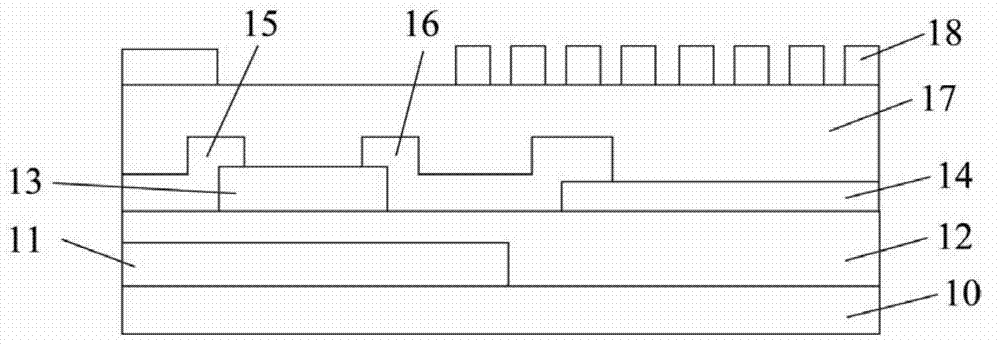
[0032] In order to solve the technical problems in the prior art that the manufacturing process of the array substrate is relatively cumbersome and the production capacity is difficult to increase, an embodiment of the present invention provides an array substrate, a display panel and a method for manufacturing the array substrate.

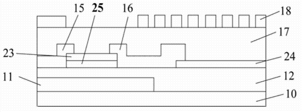
[0033] Such as Figure 6 In the illustrated embodiment, the array substrate of the present invention includes a plurality of pixel units (a cross section of a pixel unit is taken as an example in the figure), each pixel unit includes a thin film transistor, a transparent conductive metal layer 25 and a pixel electrode 24, and the thin film transistor Including gate 11, active layer 23, source 15 and drain 16, wherein,

[0034] The active layer 23 is located above or below the gate 11;

[0035] The transparent conductive metal layer 25 is in stacked contact with the active layer 23;

[0036] The source 15 and the drain 16 form a channel of the ac...


PUM


Abstract

An array substrate comprises a plurality of pixel units, and each pixel unit comprises a thin film transistor (TFT), a transparent conductive metal layer (25) and a pixel electrode (24); the TFT includes a gate electrode (11), an active layer (23), a source electrode (15) and a drain electrode (16); the active layer is disposed above or below the gate electrode; the transparent conductive metal layer makes contact with the active layer; and a channel of the active layer is defined by the source electrode and the drain electrode. A display panel and a method for manufacturing the array substrate are also disclosed.

Description

technical field [0001] The invention relates to the technical field of thin film transistor liquid crystal display, in particular to an array substrate, a display panel and a manufacturing method of the array substrate. Background technique [0002] Among flat panel display devices, Thin Film Transistor Liquid Crystal Display (TFT-LCD for short) has the characteristics of small size, low power consumption, relatively low manufacturing cost and no radiation, etc., and occupies a dominant position in the current flat panel display market. leading position. [0003] At present, the display modes of TFT-LCD mainly include TN (Twisted Nematic, twisted nematic) mode, VA (Vertical Alignment, vertical orientation) mode, IPS (In-Plane-Switching, plane direction conversion) mode and AD-SDS (ADvanced Super Dimension Switch, advanced ultra-dimensional field switching technology, referred to as ADS) mode, etc. [0004] Among them, the ADS mode liquid crystal display mainly forms a mult...

Claims


Application Information

Patent Timeline
Patent Type & Authority Patents(China)
IPC IPC(8): H01L27/02H01L29/786H01L21/77G02F1/1368
CPCG02F2001/136231H01L27/1259G02F2001/136236G02F2202/16H01L27/1288H01L27/124G02F1/1368G02F1/136231G02F1/136236G02F1/1343
Inventor 邓检
Owner BEIJING BOE OPTOELECTRONCIS TECH CO LTD
Why Eureka
Try Eureka