One-dimensional photonic crystal optical micro-cavity based on waveguide comprising low-refractive-index cores

A technology of one-dimensional photonic crystal and low refractive index, which is applied in the field of one-dimensional photonic crystal optical microcavity, can solve the problem of large size of two-dimensional photonic crystal device, and achieve the effect of compact size, simple design structure, convenient and low-cost manufacturing

Inactive Publication Date: 2013-02-06
ZHEJIANG UNIV
View PDF3 Cites 5 Cited by
  • Summary
  • Abstract
  • Description
  • Claims
  • Application Information

AI Technical Summary

Benefits of technology

This patented technology allows for smaller devices that have higher performance than previous designs due to their ability to achieve better light transmission through an interface between two different media without losing much energy during signal transferring. It achieves this by utilizing special structures made from specific material types such as silicon nitride, fluoropolymer resins, epoxy resists, etc., resulting in improved efficiency at transmitting signals over longer distances compared to traditional methods.

Problems solved by technology

This patents discuss various ways to improve the performance of optofluidic devices like diodes and amplifiers. One method involves making smaller structures called nanocapillaries, which helps increase their efficiency without requiring much energy input from external sources. Additionally, studying how these tiny structures behave when subjected to strong electromagnetic radiation allows us to study other physical phenomena related to them.

Method used


Image

  • One-dimensional photonic crystal optical micro-cavity based on waveguide comprising low-refractive-index cores
  • One-dimensional photonic crystal optical micro-cavity based on waveguide comprising low-refractive-index cores
  • One-dimensional photonic crystal optical micro-cavity based on waveguide comprising low-refractive-index cores

Examples


Embodiment 1

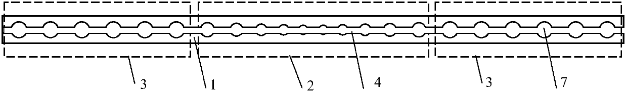
[0036] like figure 1 and Figure 7 As shown, the silicon-on-insulator (SOI) material with a top silicon thickness of 280 nm and a silicon oxide buried layer of 2 μm was used. The silicon strip waveguide with a width of 500 nm and a slit width of 100 nm and a one-dimensional periodic circular hole were fabricated by dry etching of silicon. In the periodic lattice constant area, the periodic lattice of the photonic crystal is a=480nm, and the radius r=0.28a. In the graded lattice constant area, the lattice constant decreases linearly from a to the minimum lattice constant a in the center of the microcavity through 5 times. 5 =320nm, the minimum hole radius is r 5 =0.28a 5 .

[0037] The optical microcavity in the above embodiment can support the extremely small mode volume V(~ ) and high Q (>10 3 ) , the fabrication of the entire device can be completed with only one etching.

Embodiment 2

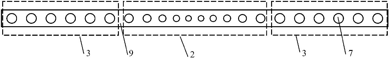
[0039] like figure 2 and Figure 8As shown, silicon-on-insulator layer with a thickness of 200nm on the top layer of silicon is selected as the material, and the horizontal slit is made by first depositing a layer of silicon dioxide with a thickness of 50nm on the silicon layer, and then depositing A silicon layer with a thickness of 200 nm is deposited or bonded on the silicon dioxide layer. After cleaning the wafer surface, perform deep ultraviolet lithography or electron beam direct writing lithography to obtain an etching mask, and dry-etch to produce silicon-silicon dioxide with a width of 500 nm and a slit width of 100 nm. —Strip waveguide with silicon three-layer structure and one-dimensional periodic circular holes. Finally, the silicon dioxide layer with low refractive index can be removed by wet etching to form an air bridge structure. In the periodic lattice constant area, the periodic lattice of the photonic crystal is a=480nm, and the radius r=0.28a. In the gra...

Embodiment 3

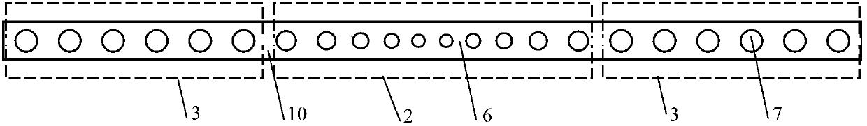
[0042] Such as image 3 and Figure 9 As shown, silicon on the insulating layer with a top silicon thickness of 250nm is selected as the material. After the wafer surface is cleaned, electron beam direct writing lithography is performed to obtain a silicon etching mask, and silicon dry etching is used to produce a 50mm wide nm, a rectangular groove with a height of 50 nm. A mask is used to deposit and fill silicon dioxide in the rectangular groove, and after a polishing process, a silicon layer with a thickness of 200 nm is deposited on the surface. After cleaning the wafer surface, perform deep ultraviolet lithography or electron beam direct writing lithography to obtain a silicon etching mask. Through silicon dry etching, a silicon strip waveguide with a width of 500 nm and a one-dimensional waveguide on the waveguide are fabricated. Periodic circular holes, and finally the silicon dioxide layer with low refractive index can be removed by wet etching to form a rectangular ...


PUM

PropertyMeasurementUnit
Thicknessaaaaaaaaaa
Thicknessaaaaaaaaaa

Abstract

The invention discloses a one-dimensional photonic crystal optical micro-cavity based on a waveguide comprising low-refractive-index cores. The one-dimensional photonic crystal optical micro-cavity is manufactured on the waveguide comprising the low-refractive-index cores, the waveguide is high in refractive index contrast, the one-dimensional photonic crystal optical micro-cavity comprises a region with a gradient lattice constant and regions with periodic lattice constants, the region with the gradient lattice constant is positioned in the center of a micro-cavity, the lattice constant of the region with the gradient lattice constant is symmetrically and linearly increased from the middle of the micro-cavity to two sides of the micro-cavity, and the regions with the periodic lattice constants are positioned on two sides of the region with the gradient lattice constant. The one-dimensional photonic crystal optical micro-cavity has the advantages that model are extremely small in size V owing to the characteristic that the light intensity is rapidly increased due to continuity of an electric displacement vector at interface positions of the low-refractive-index slit or hollow cores of the waveguide, and gradient transition and matching among the models are realized owing to the region with the gradient lattice constant in the center of the micro-cavity, so that an ultrahigh quality factor Q value is obtained; the one-dimensional photonic crystal optical micro-cavity is simple in structure and compact in size, can be processed by a CMOS (complementary metal oxide semiconductor) technology, is easy to integrate and expand, and can be conveniently manufactured at a low cost; and other low-refractive-index materials can be planted in the slits or hollow cores in the micro-cavity, and the one-dimensional photonic crystal optical micro-cavity can be widely applied to fields of nanometer laser devices, biochemical sensing, optical micro-fluid, optical micro-machines and the like.

Description


Claims


Application Information

Patent Timeline
Owner ZHEJIANG UNIV
Why Eureka
Try Eureka