Pixel structure, array substrate and liquid crystal display device

A technology of pixel structure and array substrate, applied in nonlinear optics, instruments, optics, etc., can solve problems such as affecting product quality and yield, poor DGS, and poor lines

Active Publication Date: 2015-07-01
BOE TECH GRP CO LTD +1
View PDF5 Cites 0 Cited by
  • Summary
  • Abstract
  • Description
  • Claims
  • Application Information

AI Technical Summary

Problems solved by technology

When the electrostatic breakdown of this parasitic capacitance occurs, it will lead to poor DGS
[0005] Of course, the above-mentioned short circuit problem caused by Electro-Static discharge (ESD for short) also exists between other signal transmission lines that may cross on the array substrate, such as between the common electrode line and the data line, the maintenance line, etc. The above phenomenon exists between the data line / gate line
[0006] For DGS and other line failures caused by ESD, the general method is to find the cause of static electricity on the equipment. In the prior art, the transmission speed of the rollers is reduced, the use of antistatic liquid is increased, and the static ion gun is added to reduce the static electricity. Input power in dry etching (Dry Etch) and other methods to solve the problem, but these cannot completely eliminate static electricity, resulting in the risk of line defects caused by ESD such as DGS and DCS.
Therefore, the pixel structure in the prior art does not provide any protective measures for at least the above-mentioned parasitic capacitance that is prone to electrostatic breakdown. Once it is broken down, it is difficult to completely repair it. Fix the problem of bad pixels, which will affect product quality and yield

Method used


Image

  • Pixel structure, array substrate and liquid crystal display device
  • Pixel structure, array substrate and liquid crystal display device
  • Pixel structure, array substrate and liquid crystal display device

Examples


Embodiment Construction

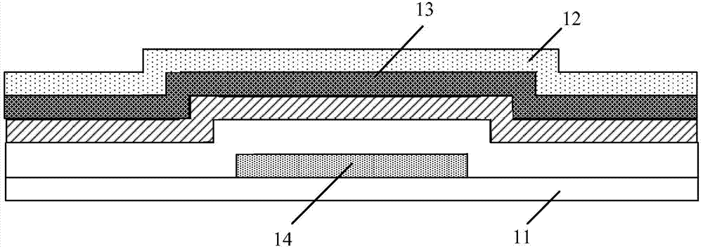
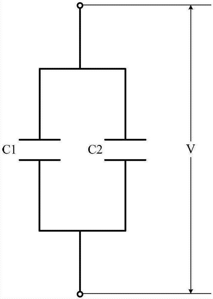
[0028] In the pixel structure, the array substrate, and the liquid crystal display device of the embodiments of the present invention, at least one protection capacitor connected in parallel with the parasitic capacitance is arranged on a certain conductive functional layer of the array substrate, so that the breakdown voltage of the protection capacitor is less than The breakdown voltage of the parasitic capacitance is used to protect the parasitic capacitance by using the protection capacitance.

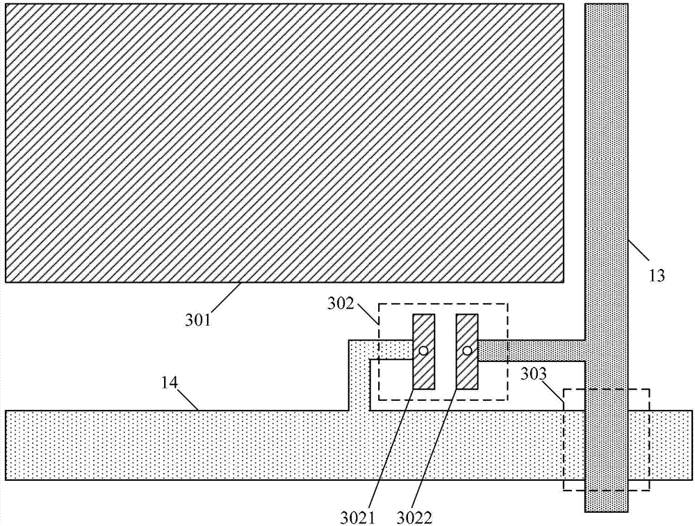
[0029] The pixel structure of the embodiment of the present invention is used for an array substrate of a thin film transistor liquid crystal display, and a plurality of functional layers are arranged on the array substrate, and the plurality of functional layers include first signal transmission lines and second signal transmission lines intersecting on different layers. Two signal transmission lines, a parasitic capacitance is formed at the intersection of the first signal transmi...


PUM


Abstract

The invention discloses a pixel structure, an array substrate and a liquid crystal display device. The pixel structure comprises a plurality of conductive function layers, wherein the function layers comprise a first signal transmission line and a second signal transmission line, which are crossly arranged in different layers; and a parasitic capacitor is formed at the crossing part of the first signal transmission line and the second signal transmission line. The pixel structure further comprises at least one protection capacitor connected in parallel with the parasitic capacitor, wherein the protection capacitor is arranged on one of the function layers, and the breakdown voltage of the protection capacitor is less than that of the parasitic capacitor. According to the invention, the parasitic capacitor between the crossed signal transmission lines is protected from breakdown.

Description

technical field [0001] The invention relates to the technical field of liquid crystal display, in particular to a pixel structure of an array substrate. Background technique [0002] Under the production conditions of the existing thin-film transistor liquid crystal display, electrostatic breakdown often occurs at the intersection of the gate line (Gate Line) and the data line (Data Line), resulting in a short circuit between the data line and the gate line (Data- Gate Short, referred to as: DGS bad). Similarly, electrostatic breakdown often occurs at the intersection of the common electrode line (Common Line) and the data line (Data Line), resulting in a short circuit between the common electrode line and the data line (Data-Common Short, referred to as: DCS failure ) [0003] Such as figure 1 As shown, it is a schematic cross-sectional view of a cross-sectional structure of a gate line and a signal line of a pixel (the cross-section is along the direction of the signal ...

Claims


Application Information

Patent Timeline
Patent Type & Authority Patents(China)
IPC IPC(8): G02F1/1362
Inventor 张明郝昭慧尹雄宣
Owner BOE TECH GRP CO LTD
Why Eureka
Try Eureka