

Organic light emitting diode pixel circuit
A technology of light-emitting diodes and pixel circuits, which is applied in the field of OLED pixel circuits, and can solve problems such as the decrease of display brightness and the rise of the critical conduction voltage of OLED components.
- Summary
- Abstract
- Description
- Claims
- Application Information
AI Technical Summary
Problems solved by technology
Method used
Image

Examples
no. 1 example
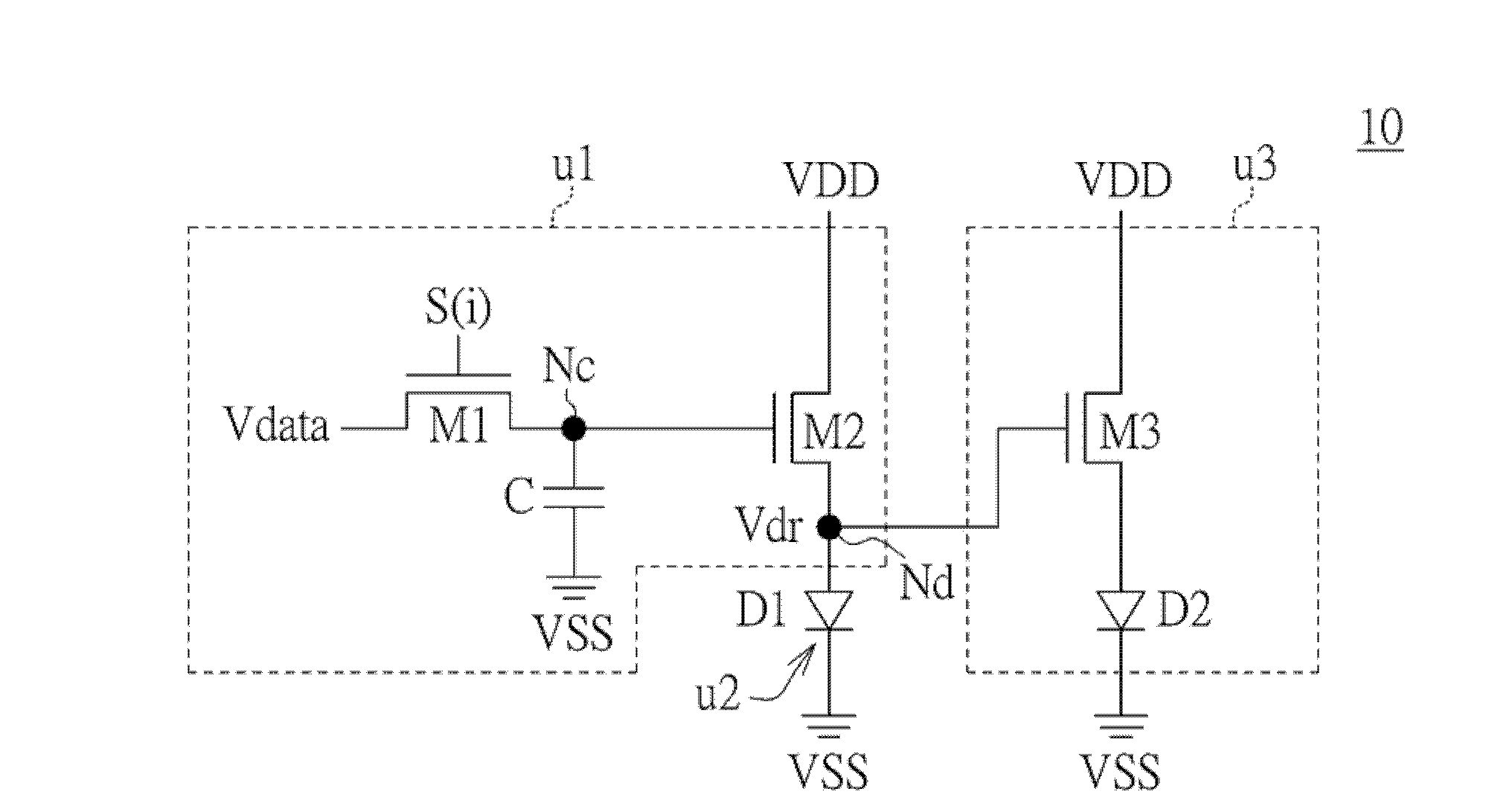
[0037] Please refer to image 3 , which shows a detailed circuit diagram of the OLED pixel circuit according to the first embodiment of the present invention. In the OLED pixel circuit 10 of this embodiment, the pixel driving unit u1 has a 2T1C circuit structure, which includes, for example, a node Nc, transistors M1, M2, and a capacitor C; the display electric element u2 includes an OLED element D1; the electric compensation unit u3 It includes a transistor M3 and an OLED element D2, wherein the OLED element D2 is used to implement a compensation electro-element, and the transistor M3 is used to implement an auxiliary driving unit.
[0038] Furthermore, the transistors M1 - M2 are, for example, N-type Metal Oxide Semiconductor (MOS) transistors. The gate of the transistor M1 receives the current scan signal S(i), the source is coupled to the node Nc, and the drain is coupled to the data line to receive the data voltage Vdata. The gate of the transistor M2 is coupled to the ...
no. 2 example
[0056] Please refer to Figure 4 , which shows a circuit diagram of an OLED pixel circuit according to a second embodiment of the present invention. The difference between the OLED pixel circuit 20 of this embodiment and the OLED pixel circuit 10 of the first embodiment is that the transistors therein adopt the LTPS process, so all of them are P-type MOS transistors.
[0057] Taking the electro-compensation unit u3 as an example, the gate of the transistor M13 receives the low-level reference voltage VSS, and the drain is coupled to the positive terminal of the OLED element D2; and the negative terminal of the OLED element D2 is connected to receive the low-level reference voltage The terminal of VSS, the source of the transistor M13 is coupled to the driving node Nd to receive the driving voltage Vdr. In this way, when the OLED pixel circuit 20 is not affected by the stress effect, the positive terminal voltage of the OLED element D1 serves as the power supply of the electro...
no. 3 example
[0061] Please refer to Figure 5 , which shows a circuit diagram of an OLED pixel circuit according to a third embodiment of the present invention. The OLED pixel circuit 30 of this embodiment is different from the OLED pixel circuit 10 of the first embodiment in that the pixel driving unit u1 has a different circuit structure. Further, the pixel driving unit u1 of this embodiment includes nodes Nc1, Nc2, transistors M21-M25 and a capacitor C, wherein the transistors M21-M25 are, for example, NMOS transistors.
[0062] The gate of the transistor M21 receives the scan signal S(i) of the current stage, the drain is coupled to the data line to receive the data voltage Vdata, and the source is coupled to the node Nc1. The gate of the transistor M22 receives the current scan signal S(i), the drain is coupled to the node Nc1 , and the source is coupled to the node Nc2 . The gate of the transistor M23 is coupled to the node Nc2 , the drain is coupled to the node Nc1 , and the sourc...
PUM
 Abstract
Description
Claims
Application Information