Led array capable of reducing uneven brightness distribution

A light-emitting array and wiring layer technology, which is applied in lighting and heating equipment, vehicle lighting systems, electrical components, etc., can solve the problems of brightness reduction, uneven brightness distribution, and interval widening, and achieve the goal of reducing uneven brightness Effect

Active Publication Date: 2013-03-06
STANLEY ELECTRIC CO LTD
View PDF8 Cites 8 Cited by
  • Summary
  • Abstract
  • Description
  • Claims
  • Application Information

AI Technical Summary

Problems solved by technology

Therefore, the injection current decreases from the right power supply side to the left and produces uneven brightness distribution
[0008] In addition, since the wiring electrodes 611 having a width of approximately 40 μm are provided between the LED elements 601, the intervals between the LED elements 601 become wide and the luminance decreases; therefore, unevenness is generated between the center and peripheral regions of the elements. Brightness distribution
If a headlight or the like is manufactured using the LED array 600 composed of the above conventional LED elements 601, uneven brightness occurs in the projected image

Method used


Image

  • Led array capable of reducing uneven brightness distribution
  • Led array capable of reducing uneven brightness distribution
  • Led array capable of reducing uneven brightness distribution

Examples


Embodiment Construction

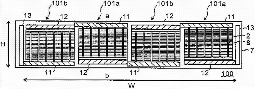
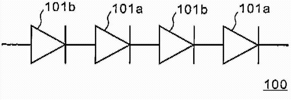
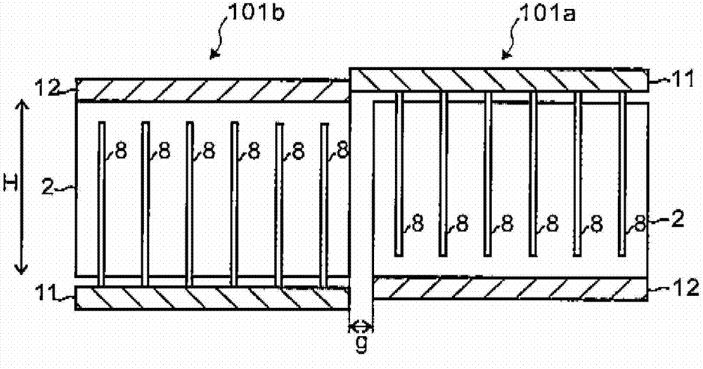
[0026] Figure 1A is a schematic plan view of an LED array 100 according to a first embodiment of the present invention, Figure 1B is a circuit diagram of the LED array 100. Figure 1C is a schematic plan view of the LED elements 101 a and 101 b constituting the LED array 100 . Figure 1D is along Figure 1A A simplified cross-sectional view of LED array 100 taken along line a-b. also, Figure 1A The hatching of the light emitting part 2 in indicates the luminance distribution, wherein an increase in density of the hatching indicates an increase in luminance.

[0027] The LED array 100 according to the first embodiment of the present invention is an array of four nitride semiconductor light emitting elements (LED elements) 101 (101a and 101b) connected in series and arranged on a support substrate 30 along the W direction in the drawing, The support substrate 30 is long in the W direction and the insulating layer 7 is formed thereon. Each of the plurality of LED element...


PUM


Abstract

The present invention relates to an LED array capable of reducing uneven brightness distribution. A semiconductor LED array comprises a plurality of semiconductor LED elements disposed on an oblong substrate that is long in a first direction and arranged along with said first direction. Each LED element comprises an electrode layer formed on the substrate, a semiconductor LED stack formed on the electrode layer, stretched long in the first direction and comprising a p-type semiconductor layer, an active layer and an n-type semiconductor layer, a first wiring layer formed along and in parallel to one long side of the semiconductor LED stack, and second wiring layers extending to a direction of a short side from the first wiring layer and electrically connected to the n-type semiconductor layer on a surface of the semiconductor LED stack. The first wiring layers are disposed on different long sides of the semiconductor LED stacks in the adjacent LED elements.

Description

field of invention [0001] The present invention relates to a semiconductor light emitting element array and a vehicle lamp using the semiconductor light emitting element array. Background technique [0002] For light emitting diode (LED) elements used in vehicle headlights, lighting equipment, etc., high power is required. If the size of the element is simply enlarged, the drive current becomes too large, and it becomes difficult to make the current flow uniformly in the element. Therefore, in order to obtain high-power LEDs, a plurality of LED elements are arranged in series to form an LED array (for example, refer to Japanese Laid-Open Patent Publication No. 2001-156331). [0003] In applications such as car headlights, oblong LED arrays are required. However, an increase in the number of LED elements is not preferable because the ratio of non-light-emitting areas between elements increases. Thus, the shape of each LED element in the LED array becomes a rectangle. [0...

Claims


Application Information

Patent Timeline
Patent Type & Authority Applications(China)
IPC IPC(8): H01L33/38H01L27/15F21S8/10F21Y101/02
CPCH01L27/153F21S48/115H01L33/385H01L33/38H01L33/0079F21S48/1159H01L33/62F21Y2101/02F21S41/147F21S41/151H01L2924/0002H01L33/0093H01L2924/00H01L33/48
Inventor 宫地护斋藤龙舞
Owner STANLEY ELECTRIC CO LTD
Why Eureka
Try Eureka