Panel module

A panel module and top surface technology, which is applied in nonlinear optics, instruments, optics, etc., can solve the problems of uneven brightness of panel modules, easy departure from the original position, and changes in spacing, etc.

Pending Publication Date: 2020-05-19
AU OPTRONICS CORP
View PDF5 Cites 0 Cited by
  • Summary
  • Abstract
  • Description
  • Claims
  • Application Information

AI Technical Summary

Problems solved by technology

[0003] After the panel module of the existing display device is bent, the spacer above the thin film transistor tends to leave its original position, that is, misalignment occurs
This misalignment will easily cause the distance between the pixel electrode layer and the second substrate to change, resulting in uneven brightness of the panel module
In addition, spacers rub against the alignment layer when misalignment occurs, resulting in broken bright spots
As can be seen from the above description, the structure of the panel module of the existing curved surface display device still needs to be improved

Method used


Image

  • Panel module
  • Panel module
  • Panel module

Examples


Embodiment Construction

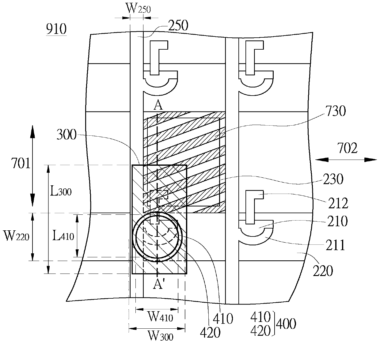
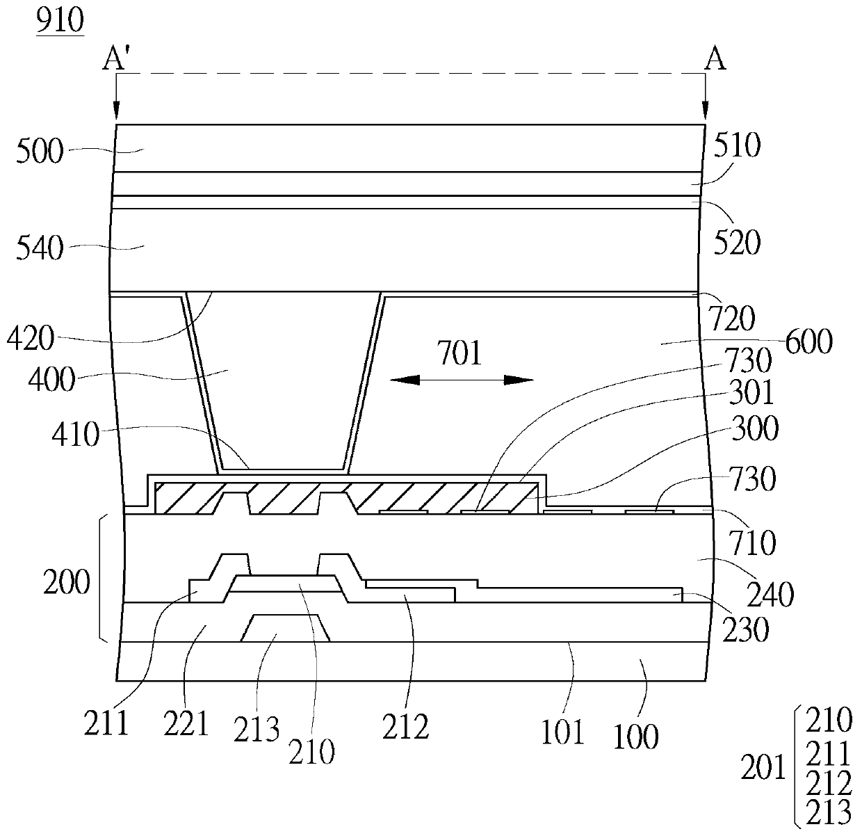
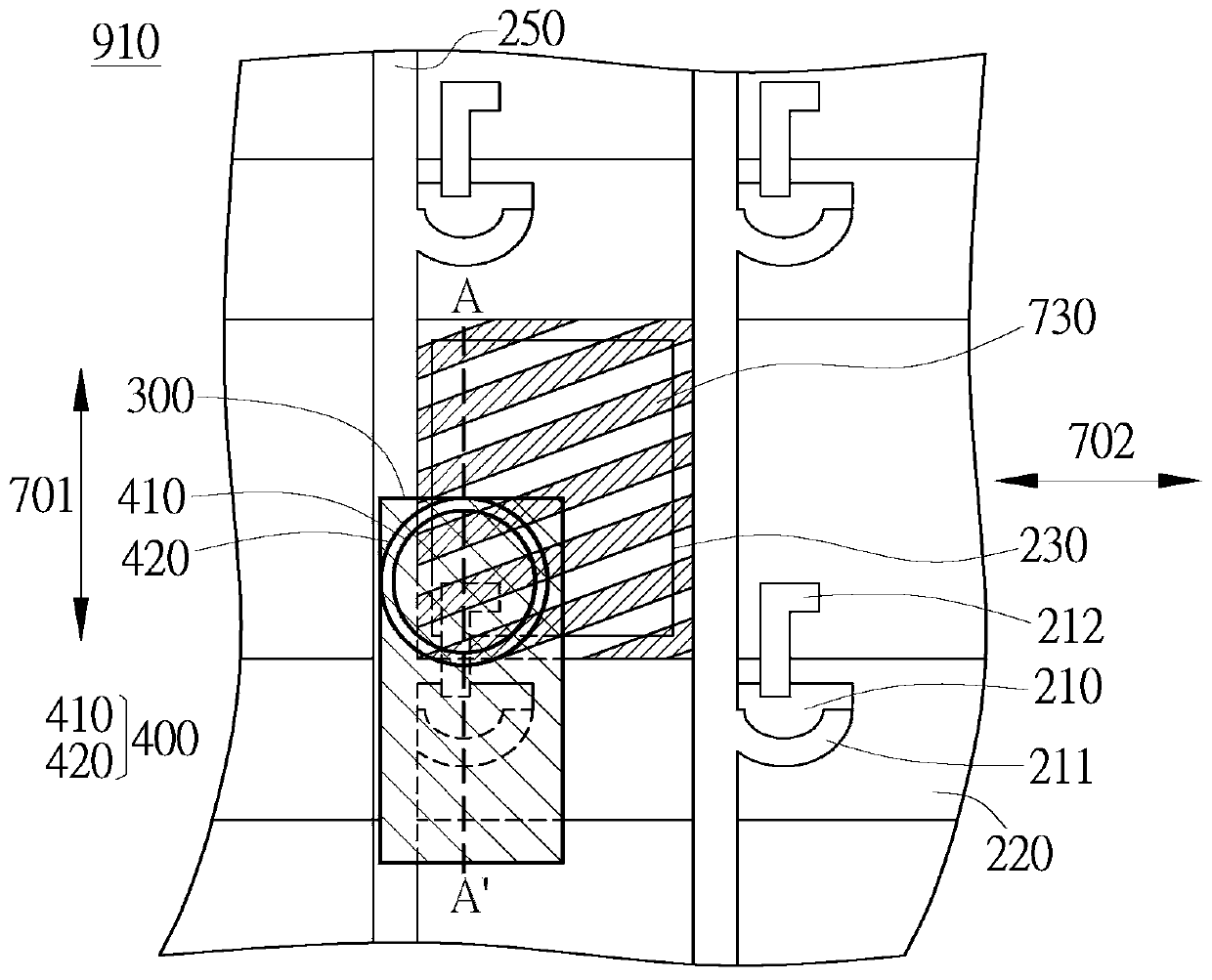
[0060] The embodiments of the connecting assembly disclosed in the present invention are described below through specific embodiments and accompanying drawings, and those skilled in the art can understand the advantages and effects of the present invention from the contents disclosed in this specification. However, the content disclosed below is not intended to limit the protection scope of the present invention, and those skilled in the art can implement the present invention with other different embodiments based on different viewpoints and applications without departing from the concept of the present invention. In the drawings, the thickness of layers, films, panels, regions, etc., are exaggerated for clarity. The same reference numerals refer to the same elements throughout the specification. It will be understood that when an element such as a layer, film, region or substrate is referred to as being "on" or "connected to" another element, it can be directly on or connect...


PUM


Abstract

A panel module comprises a first substrate, a pixel electrode layer, a plurality of protection pads, a plurality of spacers and a second substrate. The pixel electrode layer is arranged on the first top surface of the first substrate and comprises a plurality of thin film transistors. The plurality of protection pads are arranged on the pixel electrode layer. Each protection pad has a protection pad length and a protection pad width in a first direction and a second direction perpendicular to the first direction, and one side of each protection pad, which is back to the first substrate, is substantially a plane. Each spacer has a contact region disposed on one of the protective pads to contact the contact region with the protective pad. The contact area has a contact length and a contact width in the first direction and the second direction respectively, and the protection pad length and the protection pad width are larger than the contact length and the contact width respectively. Thesecond substrate is disposed opposite to the first substrate, and the spacer is disposed on the second substrate and is in contact with the protective pad. The bending amount of the panel module in the first direction is larger than that in the second direction, and the length of the protection pad is larger than the width of the protection pad.

Description

technical field [0001] The present invention relates to a panel module; in particular, the present invention relates to a panel module used for a curved display device. Background technique [0002] With the development of display technology, in addition to improvements in size and image quality, the appearance of display devices has also changed, such as curved display devices. Compared with the flat display device, the curved display device can not only be made larger in size with the same width, but also can provide a better viewing effect. For example, the TV screen can be made to be concave inward, so when the user is watching TV, the distance between the eyes and the screen will be smaller than that of the flat-screen TV, and each part of the TV and the eye line of sight are also at right angles or close to each other. The best viewing angle at right angles. [0003] After the panel module of the existing display device is bent, the spacer located above the thin film...

Claims


Application Information

Patent Timeline
Patent Type & Authority Applications(China)
IPC IPC(8): G02F1/1339G02F1/1343
CPCG02F1/1339G02F1/134309
Inventor 陈彦良
Owner AU OPTRONICS CORP
Why Eureka
Try Eureka