Current mirror circuit

A current mirror and circuit technology, applied in the direction of adjusting electrical variables, control/regulating systems, instruments, etc., can solve the problems of long time required to stabilize current and slow discharge time of NMOS tube N1, and shorten the required time and current leakage. Fast and stable effect of release ability

Active Publication Date: 2013-03-27
SHANGHAI HUAHONG GRACE SEMICON MFG CORP
View PDF5 Cites 9 Cited by
  • Summary
  • Abstract
  • Description
  • Claims
  • Application Information

AI Technical Summary

Problems solved by technology

Due to the slow discharge time of the NMOS transistor N1, it

Method used


Image

  • Current mirror circuit
  • Current mirror circuit
  • Current mirror circuit

Examples


Example

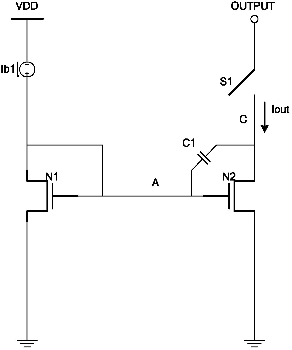
[0027] like figure 2 Shown, the first embodiment of the present invention comprises:

[0028] NMOS transistor N1, its drain is connected to the circuit power supply VDD through the constant current source Ib1, its gate is short-circuited with its drain, its gate is grounded through the capacitor C2, and its source is grounded;

[0029] NMOS transistor N2, its drain is connected to the output terminal OUTPUT through switch S1, its gate is short-circuited with its drain through capacitor C1, and its source is grounded;

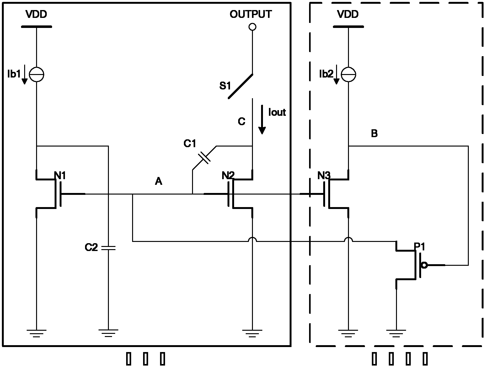
[0030] NMOS tube N3, its drain is connected to circuit power supply VDD through constant current source Ib2, its gate is connected to the gates of NMOS tube N1 and NMOS tube N2, and its source is grounded;

[0031] The source of the PMOS transistor P1 is connected to the gate of the NMOS transistor N1, the gate is connected to the drain of the NMOS transistor N3, and the drain is grounded.

[0032] When the output current is not needed, the switch S1 is turne...

Example

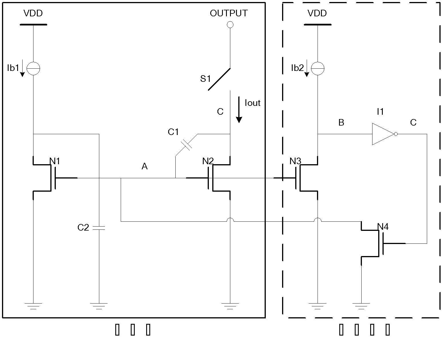
[0034] like image 3 Shown, the second embodiment of the present invention comprises:

[0035] NMOS transistor N1, its drain is connected to the circuit power supply VDD through the constant current source Ib1, its gate is short-circuited with its drain, its gate is grounded through the capacitor C2, and its source is grounded;

[0036] NMOS transistor N2, its drain is connected to the output terminal OUTPUT through switch S1, its gate is short-circuited with its drain through capacitor C1, and its source is grounded;

[0037] NMOS tube N3, its drain is connected to circuit power supply VDD through constant current source Ib2, its gate is connected to the gates of NMOS tube N1 and NMOS tube N2, and its source is grounded;

[0038] NMOS transistor N4, its drain is connected to the gate of NMOS transistor N1, its gate is connected to the drain of MOS transistor N3 through inverting amplifier I1, and its source is grounded;

[0039] The inverting amplifier I1 has its input conn...


PUM


Abstract

The invention discloses a current mirror circuit, which comprises an n-channel metal oxide semiconductor (NMOS) tube N1, an NMOS tube N2, an NMOS tube N3 and a p-channel metal oxide semiconductor (PMOS) tube P1, wherein the drain of the NMOS tube N1 is connected with a circuit voltage drain drain (VDD) through a constant current source Ib1, the grid of the NMOS tube N1 is in short-circuit connection with the drain of the NMOS tube N1, the grid of the NMOS tube N1is grounded through a capacitor C2, and the source of the NMOS tube N1 is grounded; the drain of the NMOS tube N2 is connected with the output end through a switch S1, the grid of the NMOS tube N2 is in short-circuit connection with the drain through a capacitor C1, and the source of the NMOS tube N2 is grounded; the drain of the NMOS tube N3 is connected with the circuit voltage drain drain (VDD) through a constant current source Ib2, the grid of the NMOS tube N3 is connected with grids of the NMOS tube N1 and the NMOS tube N2, and the source of the NMOS tube N3 is grounded; and the source of the PMOS tube P1 is connected with the grid of the NMOS tube N1, the grid of the PMOS tube P1 is connected with the drain of the NMOS tube N3 and the drain of the PMOS tube P1 is grounded. According to the current mirror circuit, when the voltage of a node A exceeds a certain value, the current release capacity of the node A is improved by a feedback circuit inside an accelerating circuit to quickly and steadily output current, and time for outputting steady current can be shortened.

Description

technical field [0001] The invention relates to the field of analog integrated circuits, in particular to a current mirror circuit. Background technique [0002] like figure 1 As shown, a commonly used current mirror circuit includes: constant current source Ib1, NMOS transistor N1, NMOS transistor N2 and switch S1. Wherein, the NMOS transistor N1 and the NMOS transistor N2 form a current mirror, and Ib1 is mirrored in a certain proportion to output current Iout, and the switch S1 is used to control whether to output Iout. [0003] When the output current is not needed, S1 is disconnected, and the node C voltage is 0V. When output current is needed, S1 is closed, the voltage of node C rises from 0V to OUTPUT voltage, and NMOS transistor N2 outputs current Iout at the same time. Due to the effect of the parasitic capacitances C1 and C2 of N2, when the voltage of node C rises, the voltage of node A will be pulled up at the same time, causing the current of N2 to be too larg...

Claims


Application Information

Patent Timeline
IPC IPC(8): G05F3/26
Inventor 陈涛
Owner SHANGHAI HUAHONG GRACE SEMICON MFG CORP
Why Eureka
Try Eureka