Array substrate, manufacturing method thereof, and display device
An array substrate and substrate technology, which is applied in semiconductor/solid-state device manufacturing, diodes, semiconductor devices, etc., can solve the problems of complex manufacturing process and complex hierarchical structure of microcavity structure, and achieves simple manufacturing process, low cost, and increased transparency. Overrate effect
- Summary
- Abstract
- Description
- Claims
- Application Information
AI Technical Summary
Problems solved by technology
Method used
Image

Examples
Embodiment Construction
[0062] The specific implementation manners of the present invention will be further described in detail below in conjunction with the accompanying drawings and embodiments. The following examples are used to illustrate the present invention, but are not intended to limit the scope of the present invention.
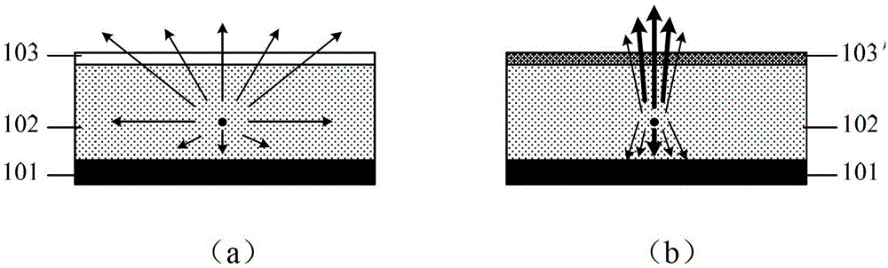
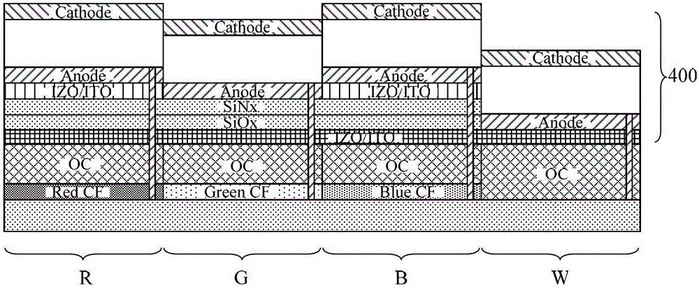
[0063] Such as Figure 5 As shown, the array substrate of this embodiment includes: a plurality of gate lines and data lines formed on the substrate 1 , and pixel units formed by intersections of the gate lines and the data lines. The pixel unit includes: a thin film transistor structure formed on the substrate and an organic light emitting diode driven by the thin film transistor structure. The organic light emitting diode is located in the pixel area of the pixel unit (usually refers to the display area other than the thin film transistor), namely Figure 5 Middle A area (areas other than area A are TFT areas). The pixel unit also includes a color filter 9 . The org...
PUM
 Abstract
Description
Claims
Application Information