Wafer pre-alignment method

A pre-alignment, wafer technology, applied in the direction of electrical components, semiconductor/solid-state device manufacturing, circuits, etc., can solve the problems of limiting the number of wafer sampling points, small sensor sampling frequency, and large space occupation

Inactive Publication Date: 2013-04-17
SHANGHAI JIAO TONG UNIV
View PDF6 Cites 34 Cited by
  • Summary
  • Abstract
  • Description
  • Claims
  • Application Information

AI Technical Summary

Problems solved by technology

This method uses the least squares circle fitting algorithm to find the center of the wafer and the center of the notch. However, the wafer contains a notch, which is not a standard circle, so the data of the notch has to be removed during calculation, which not only increases the workload, but also requires the CCD The collected wafer edge data must be evenly distributed, and the amplitude of the collected adjacent data cannot change too much, which requires high precision of hardware equipment
[0006] The pre-alignment positioning methods used above all use linear CCD sensors to detect the edge of the wafer, and the sampling frequency of this sensor is small, which limits the number of sampling points for a round of the wafer, and its space occupation is large, and the entire pre-alignment device When the space size is limited, the space size of the CCD sensor often cannot meet the requirements

Method used


Image

  • Wafer pre-alignment method
  • Wafer pre-alignment method
  • Wafer pre-alignment method

Examples


Embodiment Construction

[0052] The present invention will be described in detail below in conjunction with specific embodiments. The following examples will help those skilled in the art to further understand the present invention, but do not limit the present invention in any form. It should be pointed out that for those of ordinary skill in the art, a number of modifications and improvements can be made without departing from the concept of the present invention. These all belong to the protection scope of the present invention.

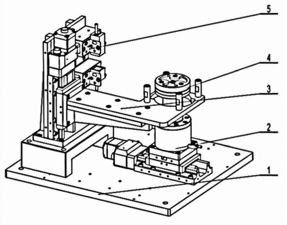
[0053] Such as figure 1 As shown, it is a wafer pre-alignment device capable of implementing the method provided by the present invention. The wafer pre-alignment device includes a working table 1, a θ-Y two-degree-of-freedom movement unit 2, a vertical transition unit 3, and a vacuum suction unit 4. Visual inspection unit 5, data acquisition unit 6 and motion control unit 7. Wherein: the θ-Y two-degree-of-freedom motion unit 2 is used to adjust the eccentricity and notch...


PUM


Abstract

The invention provides a wafer pre-alignment method, which comprises the following steps of: calculating shape center position coordinates of a wafer, radial displacement maximum offset emax and an included angle of a radial displacement maximum offset part and horizontal Y direction by using a high-accuracy laser transmitting sensor according to one-circumference data of the edge of the wafer; driving the wafer to rotate at an angle so as to position the radial displacement maximum offset emax and the horizontal Y direction on a straight line, thereby finishing shape center positioning of the wafer; and accurately positioning a notch of the wafer according to a shape center algorithm. According to the wafer pre-alignment method, the edge of the wafer is detected by using a light transmitting sensor, and the positions of a shape center and the notch of the wafer are determined by using the shape center algorithm, so that the accuracy of the positioning method is effectively improved, the time and the space occupied by a pre-alignment are reduced, and the cost is reduced.

Description

Technical field [0001] The invention relates to semiconductor manufacturing, in particular to a wafer pre-alignment method. Background technique [0002] With the development of photolithography technology, higher requirements are put forward for the accuracy of wafer alignment and exposure systems. In order to shorten the time for the precise alignment of the random search mark position and improve the utilization rate of the wafer, it is necessary to add a pre-alignment process in the wafer transfer stage before the precise alignment to ensure the accurate alignment of the wafer in a short time . [0003] At present, the pre-alignment of wafers has developed from the initial mechanical pre-alignment to optical pre-alignment, and the accuracy has also been increased from 200 microns to 1 micron or even sub-micron, and high productivity is required. Therefore, high requirements are placed on the detection, manufacturing and installation accuracy of the pre-alignment device. The ...

Claims


Application Information

Patent Timeline
Patent Type & Authority Applications(China)
IPC IPC(8): H01L21/68
CPCH01L21/681
Inventor 张波刘品宽朱晓博张帆梁家欣
Owner SHANGHAI JIAO TONG UNIV
Why Eureka
Try Eureka