Silicon sheet pre-positioning system based on multiple sensor data fusing

A data fusion, multi-sensor technology, applied in the system field of semiconductor lithography technology, can solve the problems of CCD sensor space size unable to meet requirements, limited space for accuracy improvement, low sensor sampling frequency, etc., to achieve high repeatability accuracy, The effect of improving accuracy and improving overall performance

Inactive Publication Date: 2009-02-04
SHANGHAI JIAO TONG UNIV
View PDF6 Cites 0 Cited by
  • Summary
  • Abstract
  • Description
  • Claims
  • Application Information

AI Technical Summary

Problems solved by technology

The system uses the least squares circle fitting algorithm to find the center of the silicon wafer and the center of the notch. However, the silicon wafer contains a notch, which is not a standard circle, so only part of the data of the notch can be removed during calculation.
In addition, the rough positioning of the notch directly determines the start and end points of the fine sampling of the notch, while the rough positioning of the notch using the edge change rate method has poor precision, which directly affects the fine positioning of the notch
[0005] The common limitations of the above-mentioned pre-positioning systems are: (1) Linear CCD sensors are used to detect the edge of silicon wafers, and the sampling frequency of this sensor is relatively small, which directly limits the number of sampling points in a week, thus limiting the room for accuracy improvement
(2) The linear CCD sensor takes up a lot of space, and the space size of the CCD sensor cannot meet the requirements when the space size of the host frame is limited
This adjustment method not only leads to surface contact and particle generation, but also takes a long time to adjust. In addition, the silicon wafer will produce a slight offset during the switching process, resulting in the introduction of errors.

Method used


Image

  • Silicon sheet pre-positioning system based on multiple sensor data fusing

Examples


Embodiment Construction

[0019] The embodiments of the present invention are described in detail below in conjunction with the accompanying drawings: this embodiment is implemented under the premise of the technical solution of the present invention, and detailed implementation methods and processes are provided, but the protection scope of the present invention is not limited to the following implementations example.

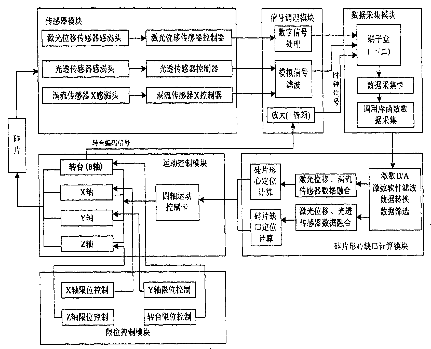
[0020] Such as figure 1 As shown, this embodiment includes six modules: a sensor module, a signal conditioning module, a data acquisition module, a silicon wafer centroid gap calculation module, a motion control module, and a limit control module. The sensor module connects the detected silicon chip information to the signal conditioning module, the signal conditioning module recuperates the silicon chip information after receiving it, the conditioned signal is connected to the data acquisition module, and the data acquisition module converts the signal conditioned by the signal condit...


PUM


Abstract

This invention relates to a pre-location systm for silicon chips combined by multiple sensor data, in which, a sensor module connects detected Si chip information to a signal regulation module to regulate it then to be connected to a data collecting module to convert the signals to data and output them to a chip like core notch computation module to process the data to get the regulation volume of a movement control module to be output to it to finish the actual operation for locating the chip, a limit control module diagnoses limits and eliminates fault for the movement control module, which outputs part signals to a signal process module to provide outer clock signal for the data collection module.

Description

technical field [0001] The invention relates to a system in the technical field of semiconductor lithography, in particular to a silicon wafer pre-positioning system based on multi-sensor data fusion. Background technique [0002] When the lithography machine develops to the nanometer level, it is required that the silicon wafers transported by the silicon wafer transmission system must meet the repeatability positioning requirements of the micron level, and the silicon wafer pre-positioning system is what completes the positioning in the silicon wafer transmission system. The silicon wafers are randomly placed in the cassette. Due to the gap between the cassettes, the silicon wafers have a random eccentricity of ±2mm and a random notch direction. The pre-positioning table must adjust the random eccentricity and notch direction of the silicon wafer to complete micron-level positioning. The equipment required for the silicon wafer pre-positioning system generally includes th...

Claims


Application Information

Patent Timeline
Patent Type & Authority Patents(China)
IPC IPC(8): H01L21/68G03F7/20G03F9/00
Inventor 曹其新黄春霞刘仁强王美玲
Owner SHANGHAI JIAO TONG UNIV
Why Eureka
Try Eureka