Device and method for generating double-layer plasma photon crystal

A plasma and photonic crystal technology, applied in the field of plasma application technology and optics, can solve the problems of limited application fields and application prospects, limited wavelength range of light modulation, single modulation method, etc., to achieve diversification and broaden the wavelength band. , the effect of a wide range of application fields and application prospects

Inactive Publication Date: 2015-04-01
HEBEI UNIVERSITY
View PDF5 Cites 0 Cited by
  • Summary
  • Abstract
  • Description
  • Claims
  • Application Information

AI Technical Summary

Problems solved by technology

[0004] Prior patents ZL200610102333.0 and ZL201010523218.7 have realized plasmonic photonic crystals with three and four refractive indices by adjusting experimental conditions, but they can only be devices for generating single-layer plasmonic photonic crystals, and single-layer plasmonic crystals The modulation of light by bulk photonic crystals is still very limited in the wavelength range, and because of the single modulation method, it is also limited in application fields and application prospects.

Method used


Image

  • Device and method for generating double-layer plasma photon crystal
  • Device and method for generating double-layer plasma photon crystal
  • Device and method for generating double-layer plasma photon crystal

Examples


Embodiment 1

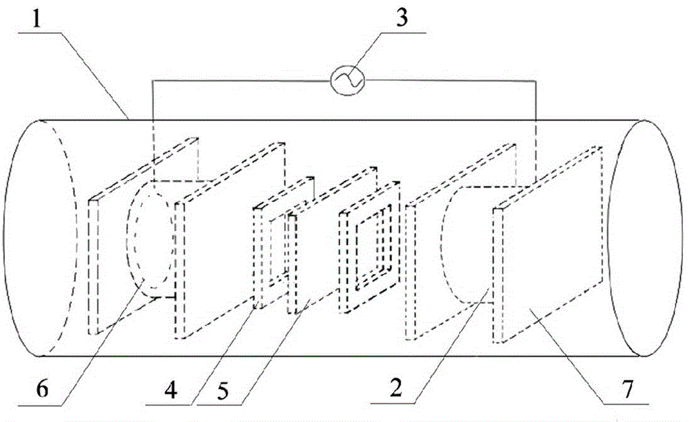
[0029] Such as figure 1 As shown, the device for generating double-layer plasma photonic crystals of the present invention is that two sealed dielectric containers are symmetrically arranged in a horizontal cylindrical vacuum reaction chamber 1, and the sealed dielectric container is filled with water to form two polar plates. The opposite water electrode 2. The two water electrodes 2 are electrically connected to the plasma generating power source 3. The water electrode 2 can also be a plexiglass tube, sealed with glass baffles 7 on both sides, filled with water, and a copper ring 6 is built in. The power cord of the plasma generating power supply 3 is connected to the copper ring 6. The thickness of the glass baffle 7 is between 0.1 mm and 5 mm and serves as a discharge medium. The wall of the vacuum reaction chamber 1 has an air inlet and an air outlet.

[0030] Two frames 4 with different thicknesses are arranged between the two water electrodes 2 as the boundary of the dis...

Embodiment 2

[0036] The method for producing a photonic crystal with double-layer plasma in the present invention is as follows: a vacuum reaction chamber 1 is provided, an air inlet and an air outlet are opened on the wall, and two water electrodes with opposite polar plates are arranged in the vacuum reaction chamber 1 2. The water electrode 2 uses a plexiglass tube sealed with glass baffles 7 on both sides and filled with water, and a built-in copper ring 6 is electrically connected to the plasma generating power supply 3. Among them, water is used as an electrode, and a glass baffle 7 with a thickness between 0.1 and 5 mm is used as a discharge medium. Two frames 4 with different thicknesses are arranged between the two water electrodes 2 as the boundaries of the discharge air gap, and the frame 4 has a thickness between 0.1 mm and 20 mm. A dielectric plate 5 is arranged between the frames 4 to separate the discharge gap into two layers with adjustable thickness. In order to improve th...


PUM


Abstract

The invention relates to a device and a method for generating a double-layer plasma photon crystal. The device comprises a vacuum reaction chamber, two water electrodes and a plasma generation power supply, wherein the two water electrodes are arranged in the vacuum reaction chamber and provided with opposite pole plates; and the plasma generation power supply is electrically connected with the water electrodes. The device is characterized in that two borders with different thicknesses, which are used as the boundaries of a discharge air gap, are arranged between the two water electrodes; a dielectric plate is arranged between the two borders; and the borders and the dielectric plate are respectively perpendicular to the axial lines of the two water electrodes. According to the device and the method disclosed by the invention, the double-layer plasma photon crystal is realized for the first time; and the double-layer plasma photon crystal has the advantages of fixed lattice constant proportion and different symmetries and achieves the purpose that optical transmission is regulated by regulating lattice symmetry, so that the double-layer plasma photon crystal has wide in application field and application prospect.

Description

technical field [0001] The invention relates to a plasma application technology and an optical technology, in particular to a device and method for producing double-layer plasma photonic crystals. Background technique [0002] Photonic crystals, also known as photonic bandgap materials, are an artificial "crystal" structure formed by arranging two dielectric materials with different dielectric constants in space at a certain period (the size is on the order of the wavelength of light). The dielectric constant of a photonic crystal is a periodic function of space. If the periodic modulation of photons by the dielectric coefficient is strong enough, the photon energy propagating in the photonic crystal will also have an energy band structure, and photon "forbidden" will appear between the bands. band", photons whose frequency falls in the forbidden band cannot propagate in the crystal. The position and shape of the photonic forbidden band depend on the refractive index ratio ...

Claims


Application Information

Patent Timeline
Patent Type & Authority Patents(China)
IPC IPC(8): G02B1/00H05H1/24
Inventor 董丽芳申中凯李犇张新普
Owner HEBEI UNIVERSITY
Why Eureka
Try Eureka